HScope is in continuous development thanks to the contributions of the supporters, and aim to become one of the best affordable high-tech diagnostic tool. Support today the Research & Development!
Project material can be found here in Github, other resources at the end of this page
It is suggested to join the Telegram group to get more info and support
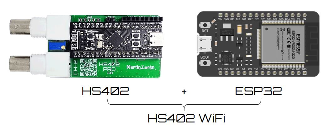
Hardware
To build the HS402-WiFi oscilloscope you can choose among these 2 options.
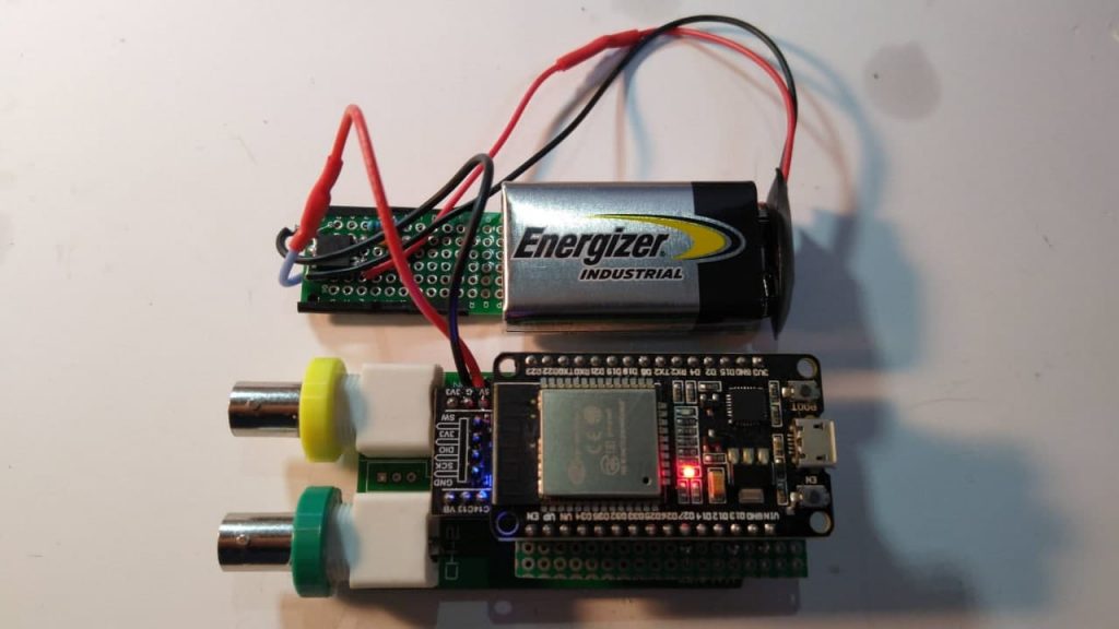
1. Easy Built
You need:
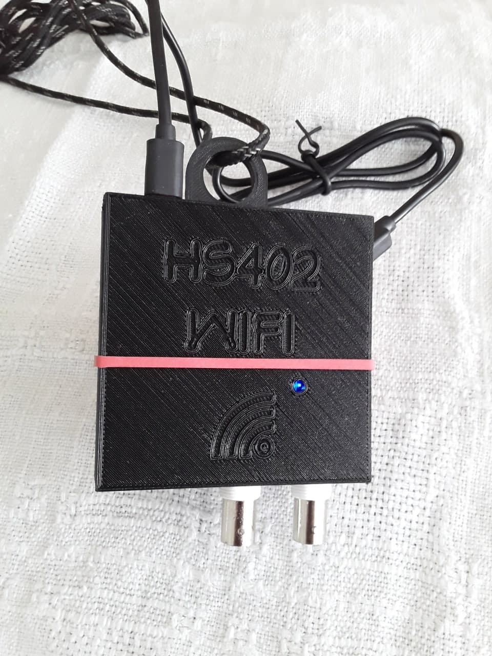
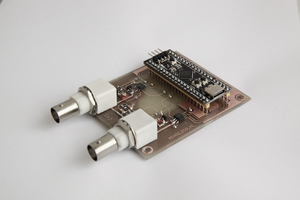
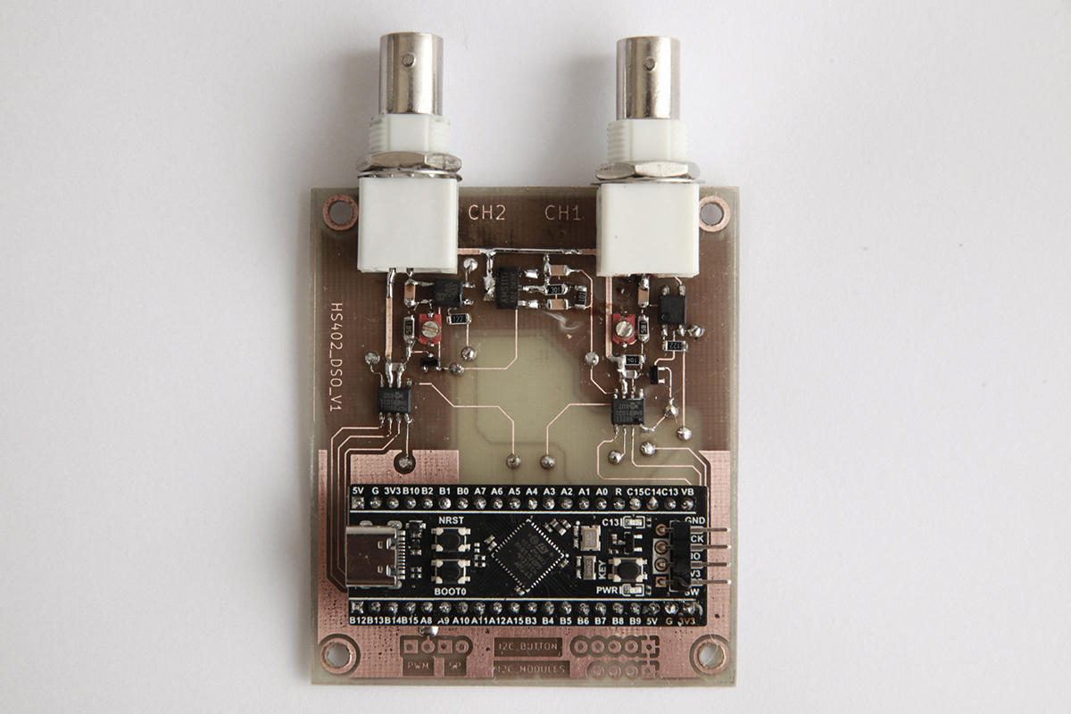
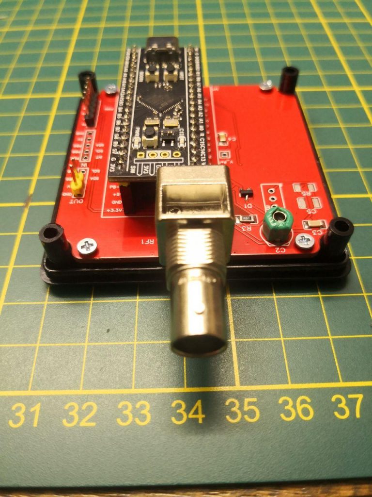
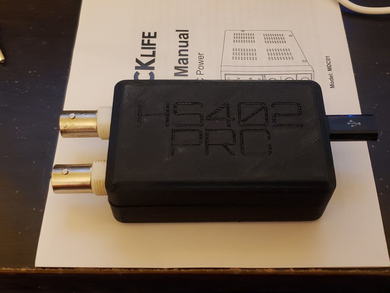
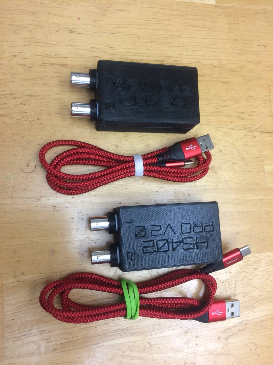
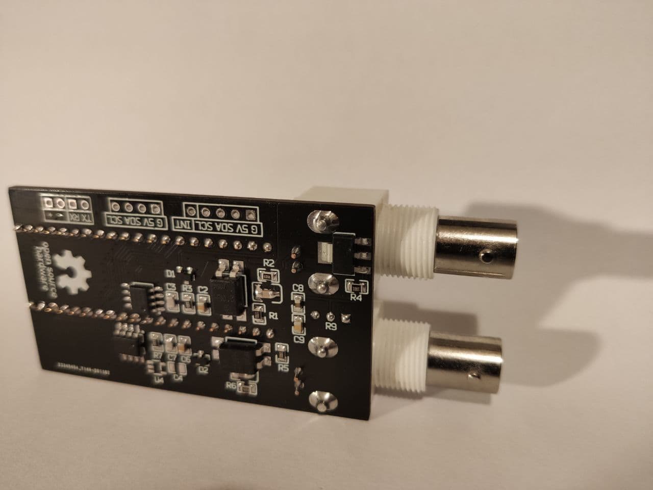
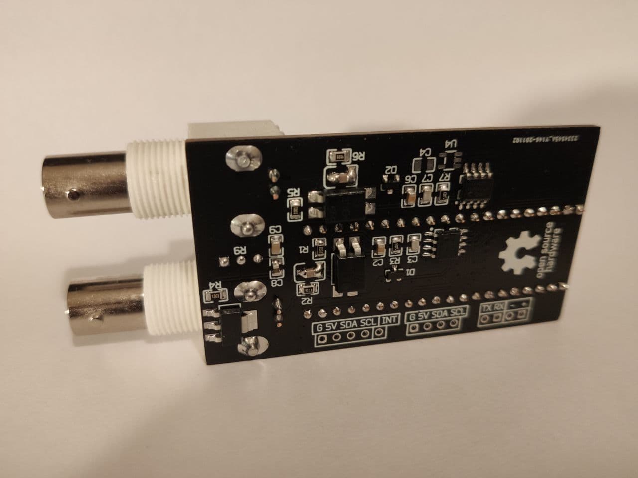
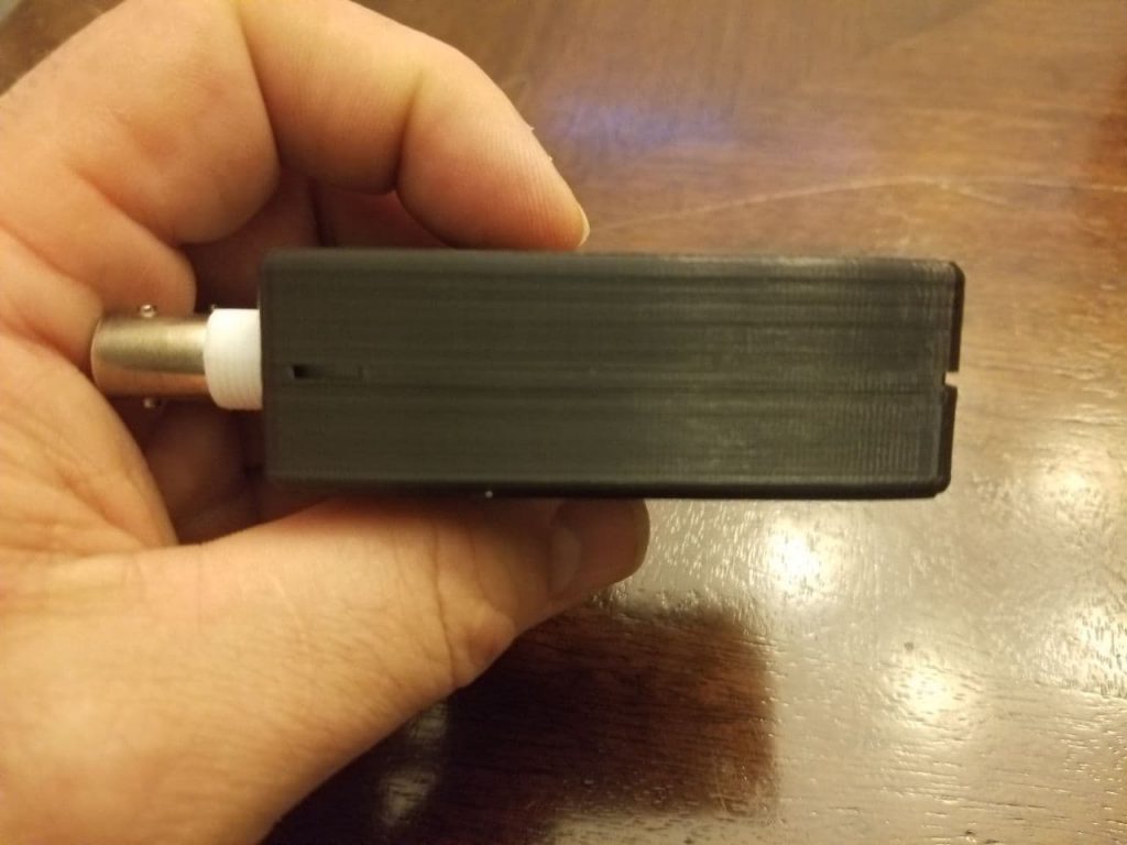
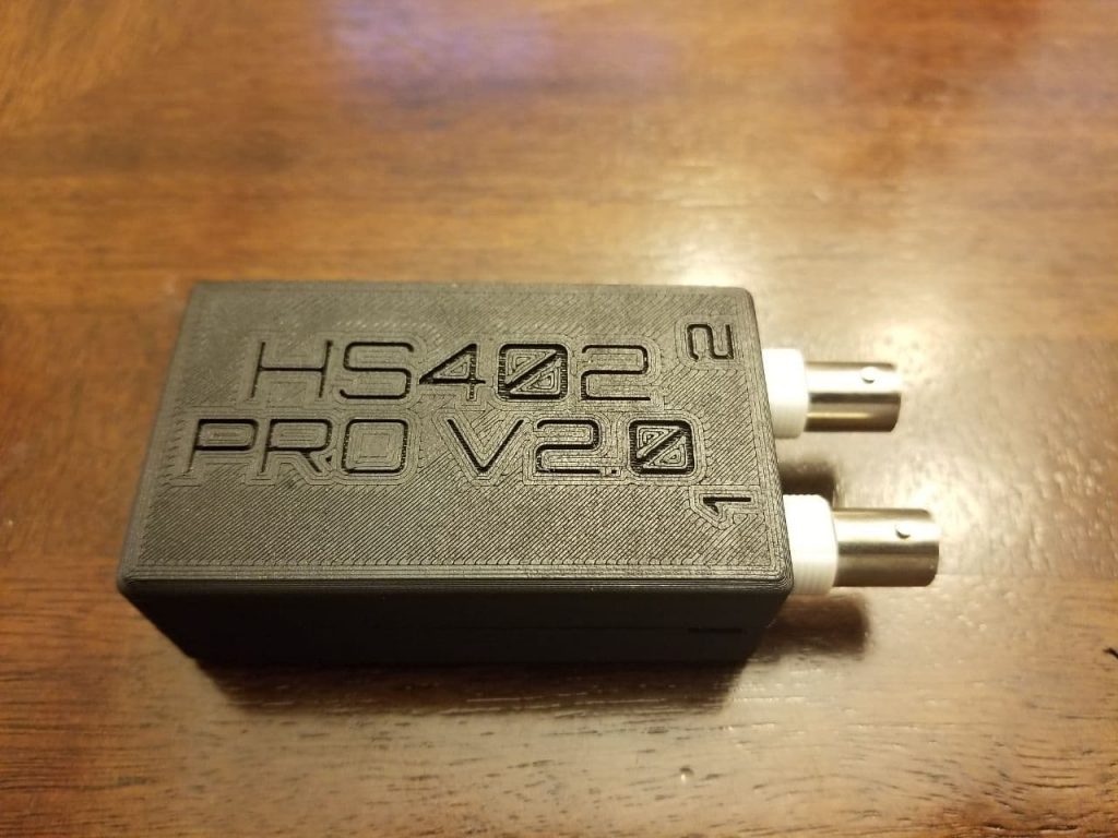
HS402 oscilloscope (built with PCB V2.0 or PCB V3.0) with Firmware ver. ≥ 1.7
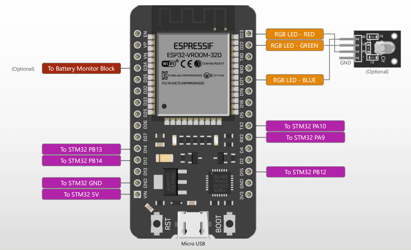
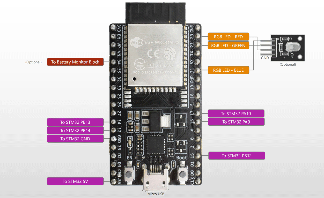
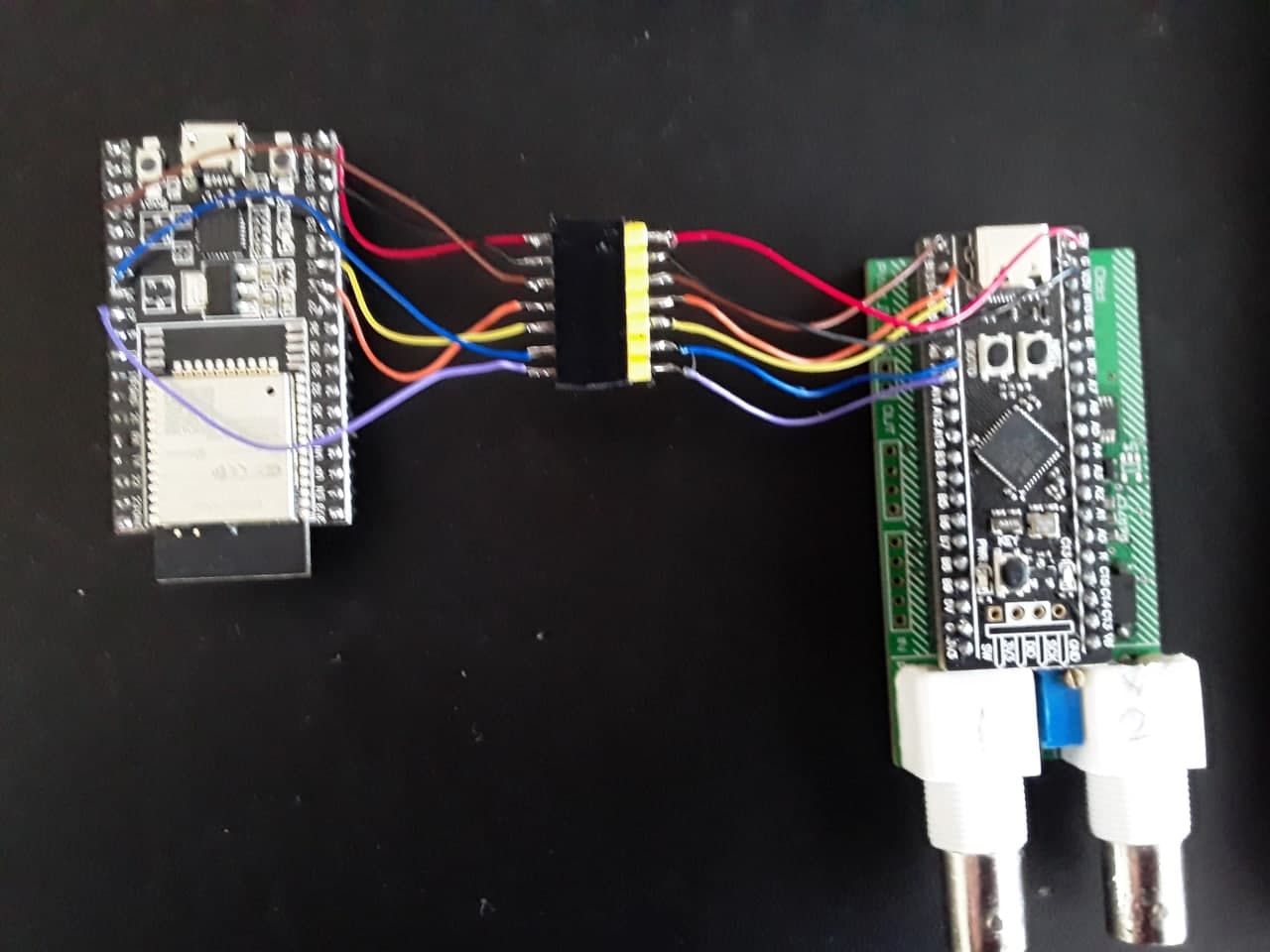
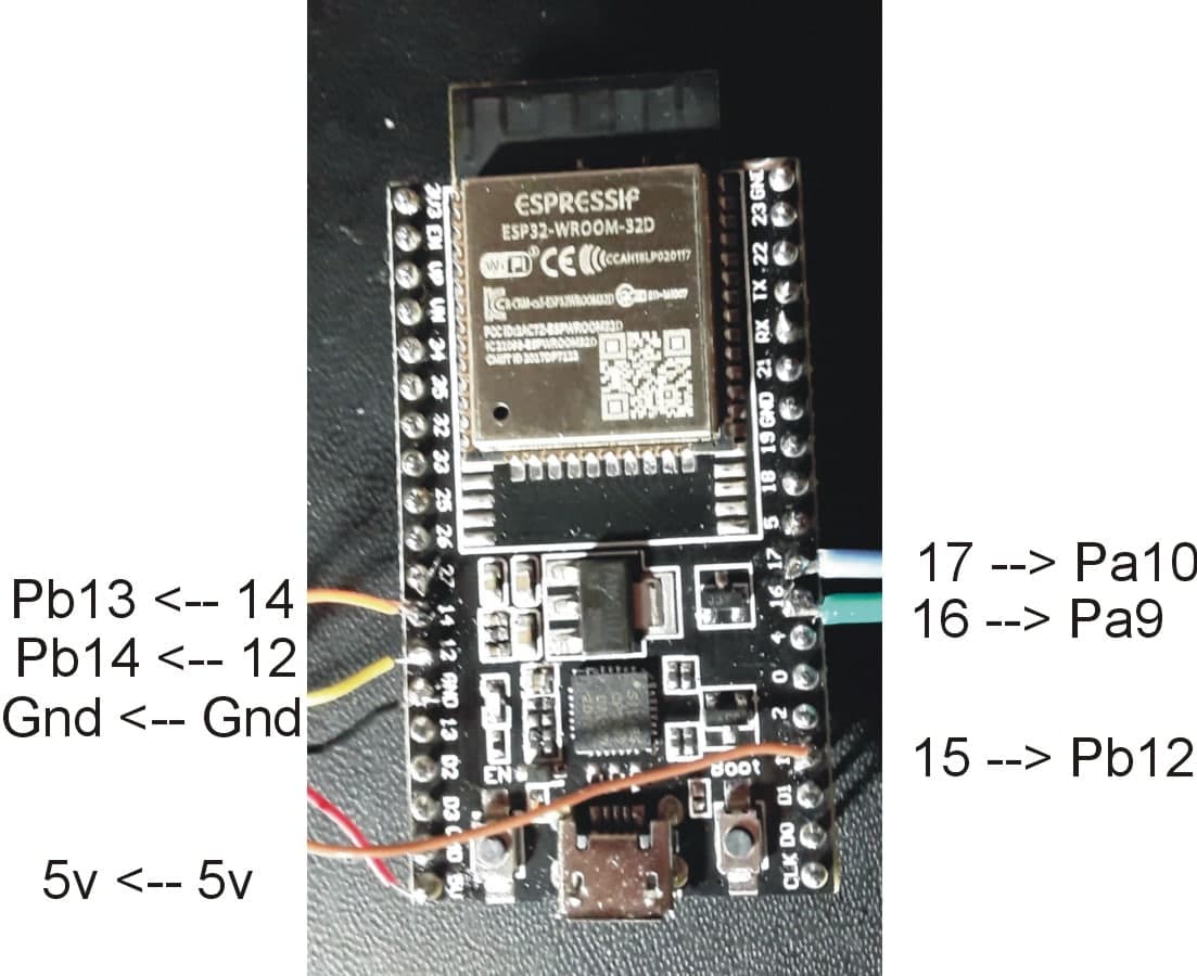
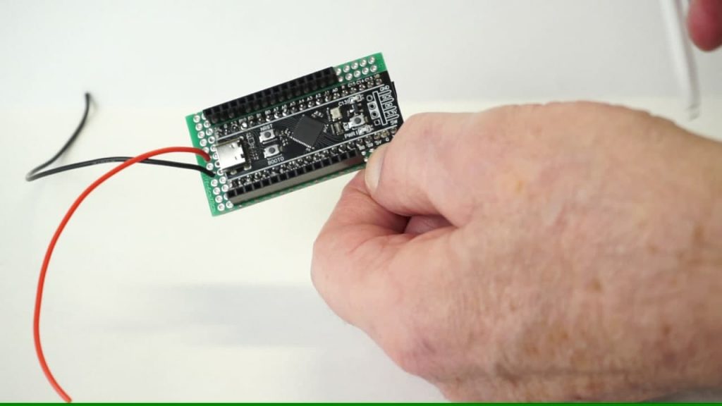
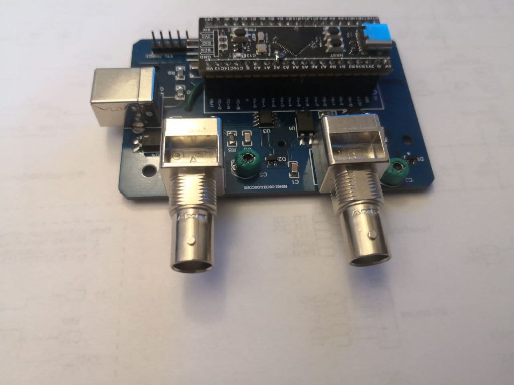
ESP32 Development board (one with ESP32-WROOM first version or ESP32-WROOM-32D), connected to STM32 as following and flashed with latest ESP32 Firmware. Flashing instructions here.
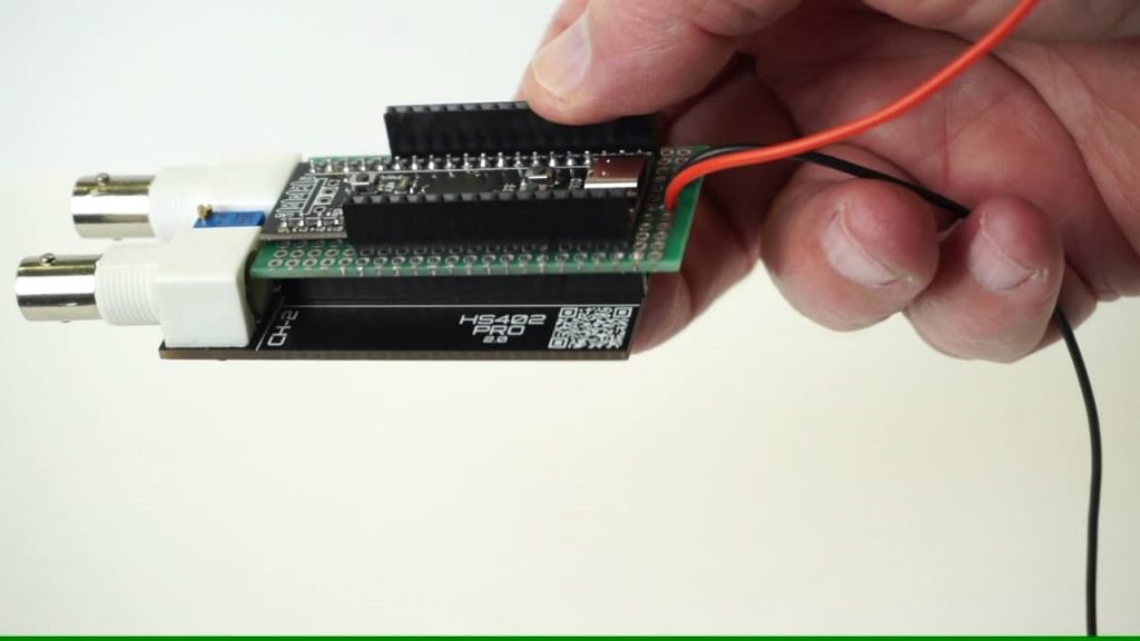
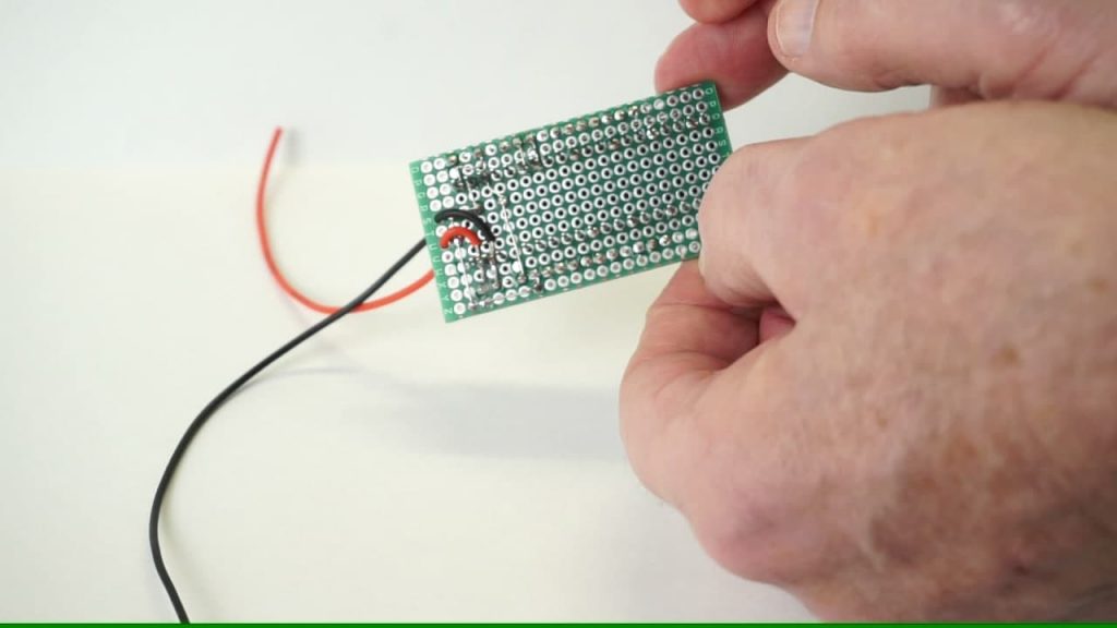
You can also use a PCB adapter created by Mikael to connect the ESP32 and STM32 together. Look at this project here, usage video here.
ESP32 board can be very different but from these schematic it could be possible to find the right pins.
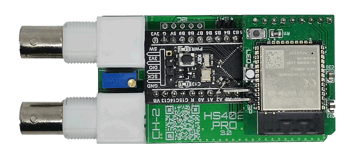
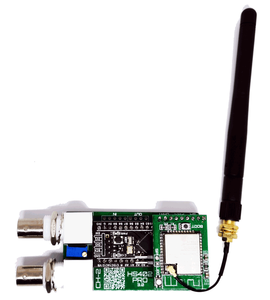
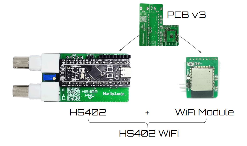
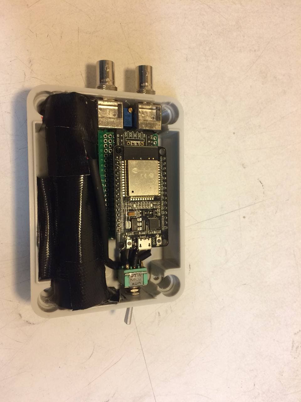
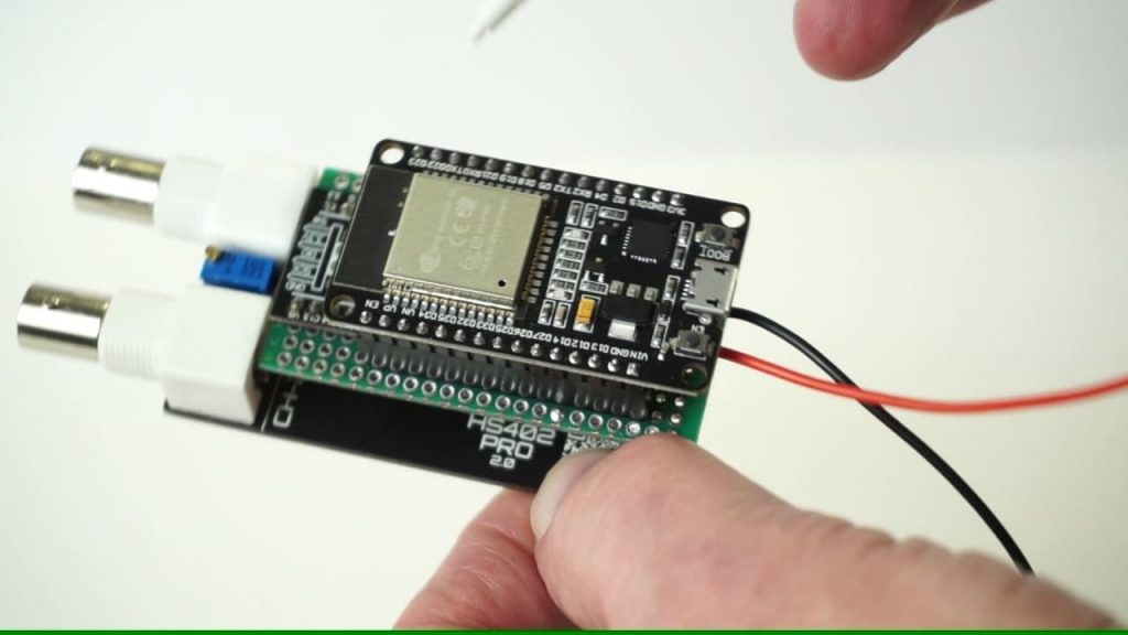
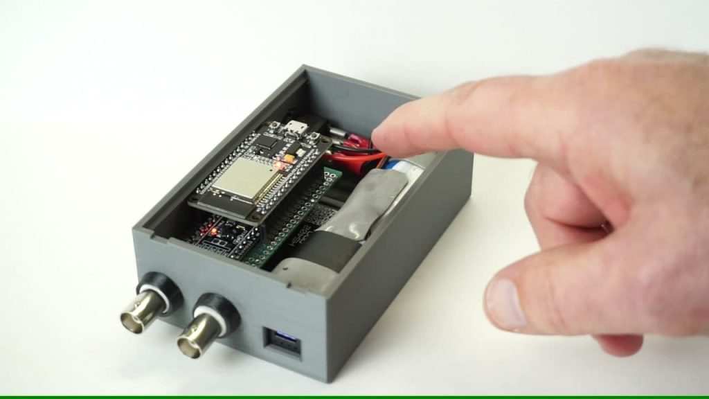
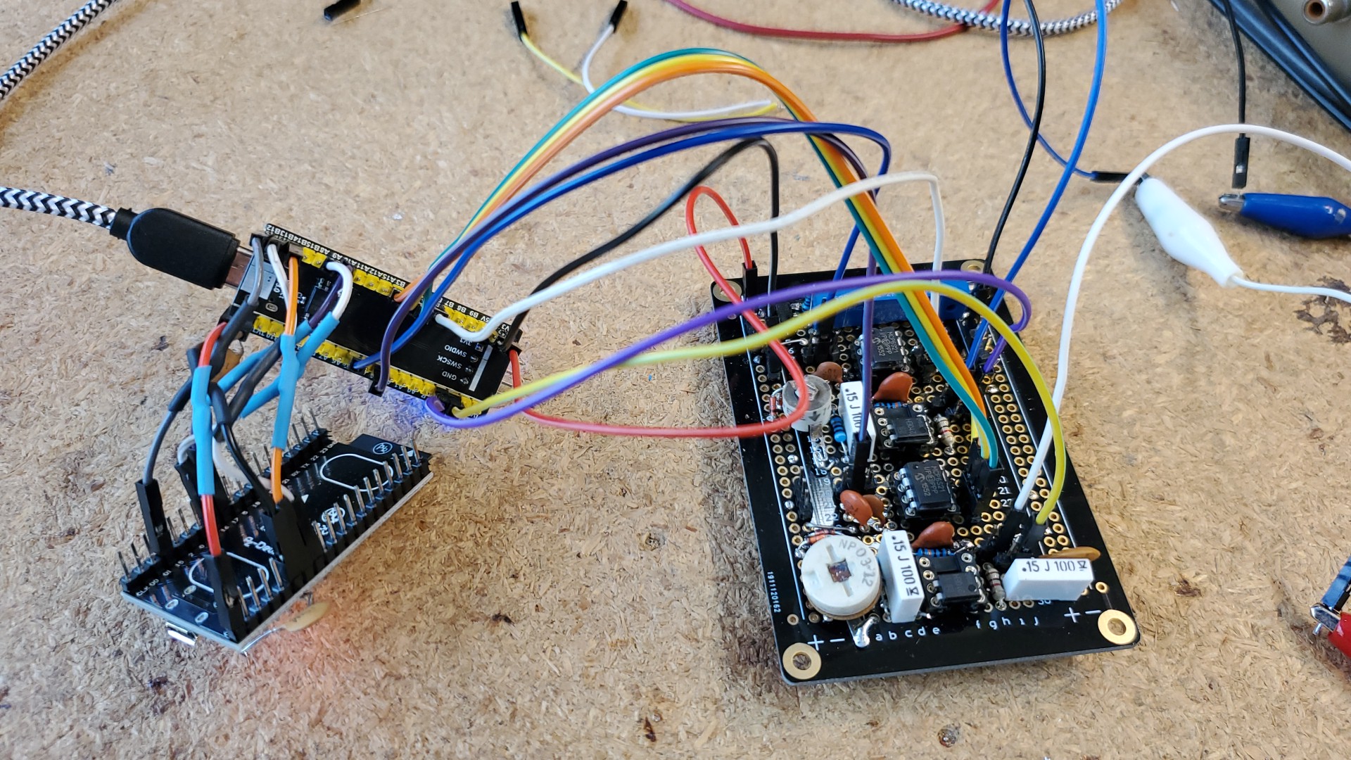
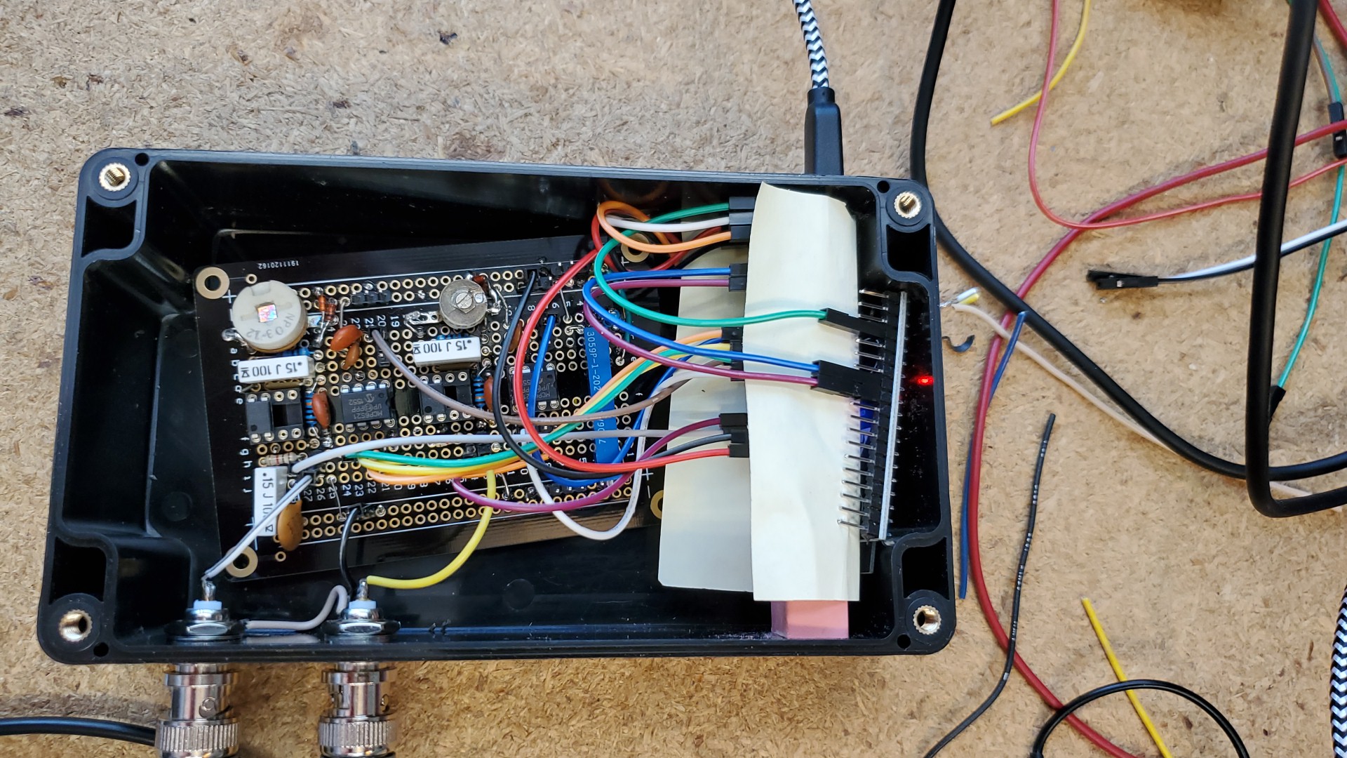
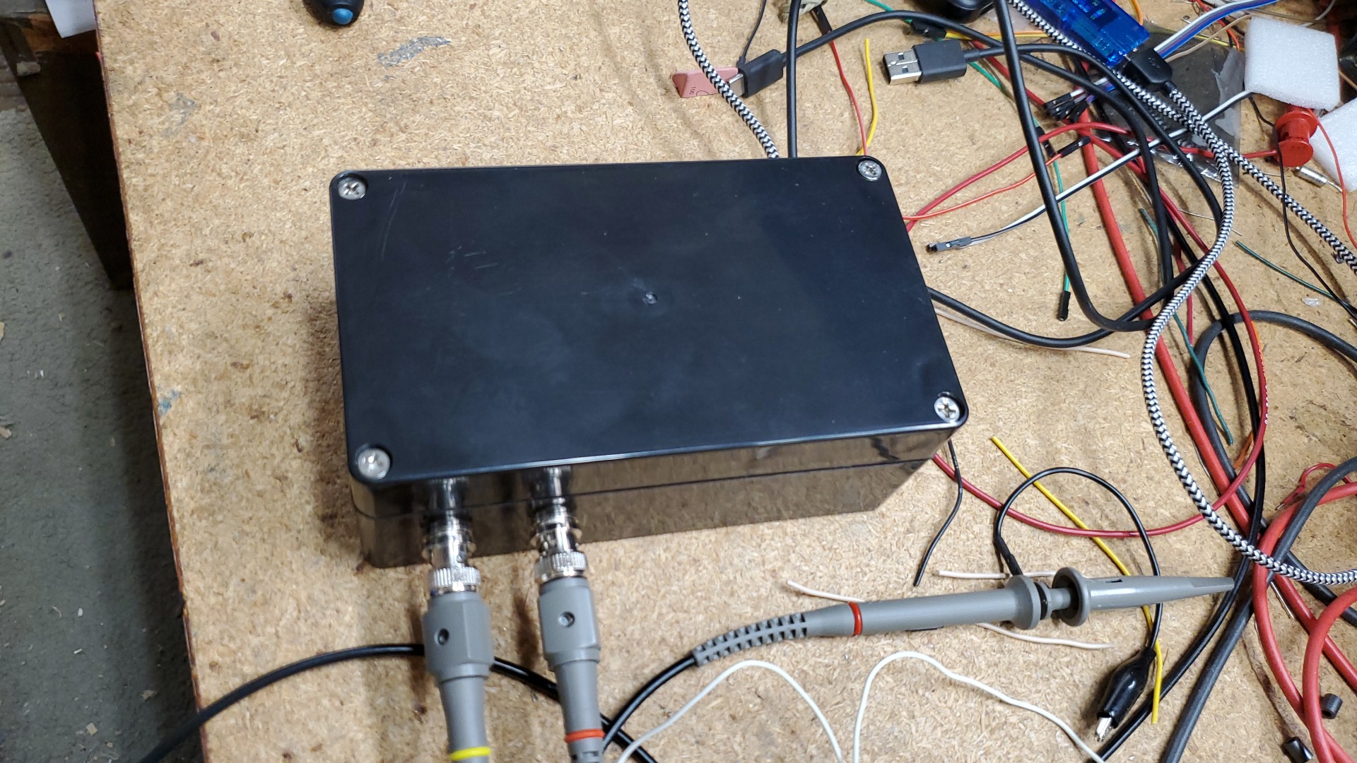
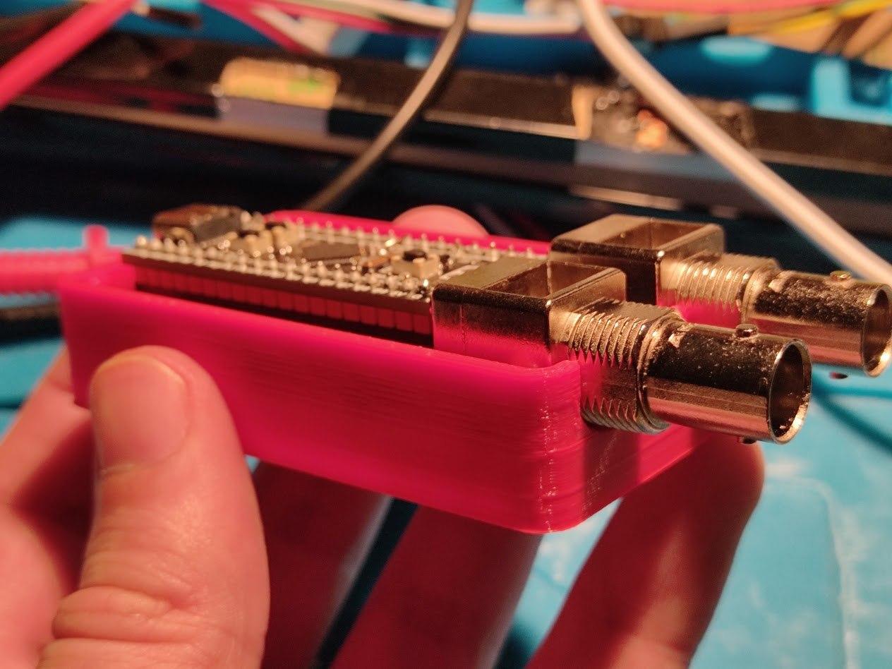
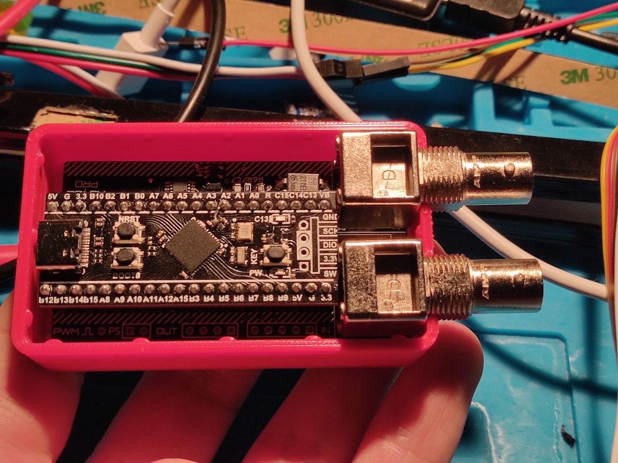
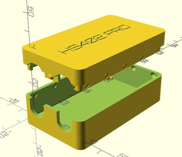
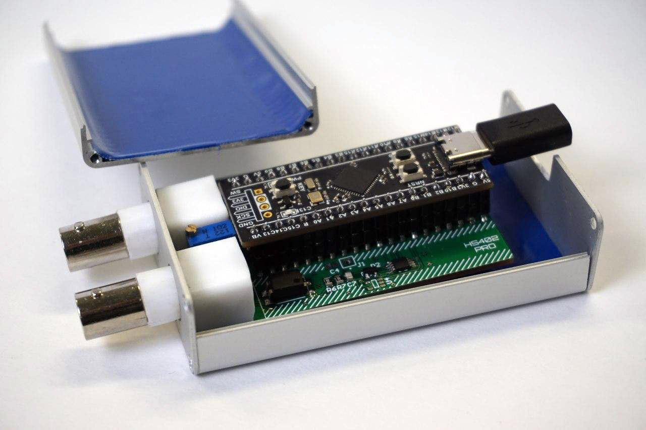
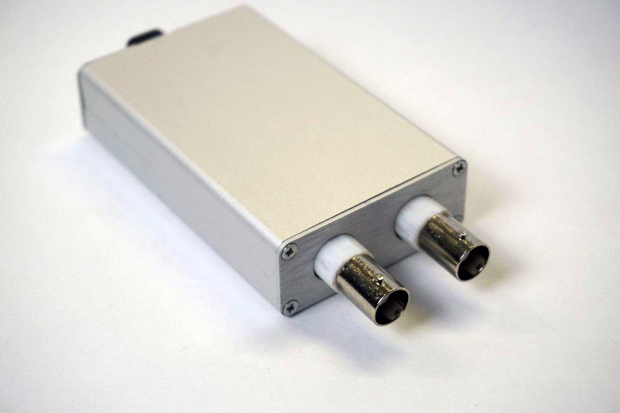
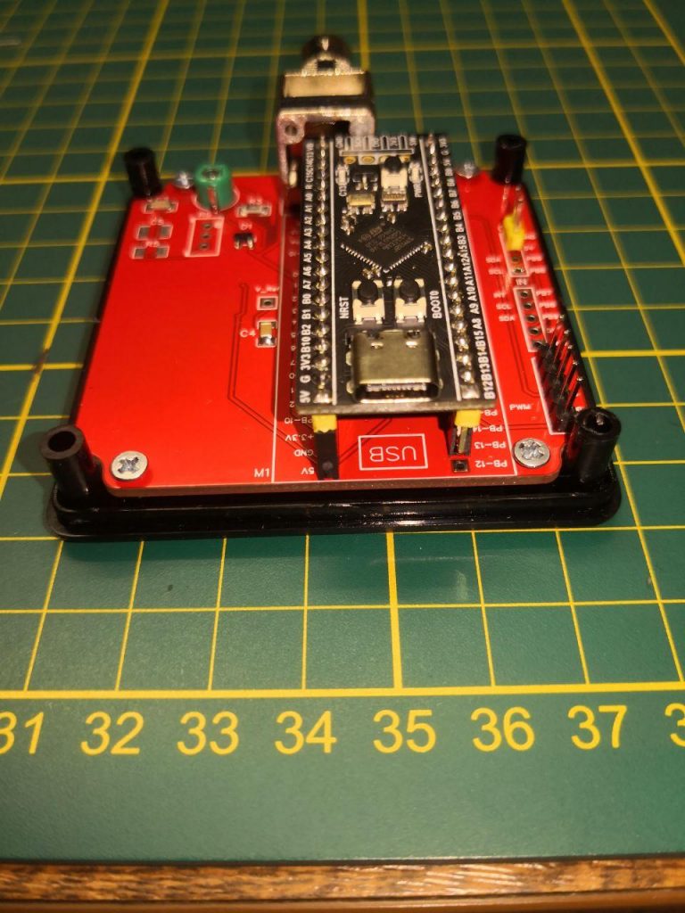
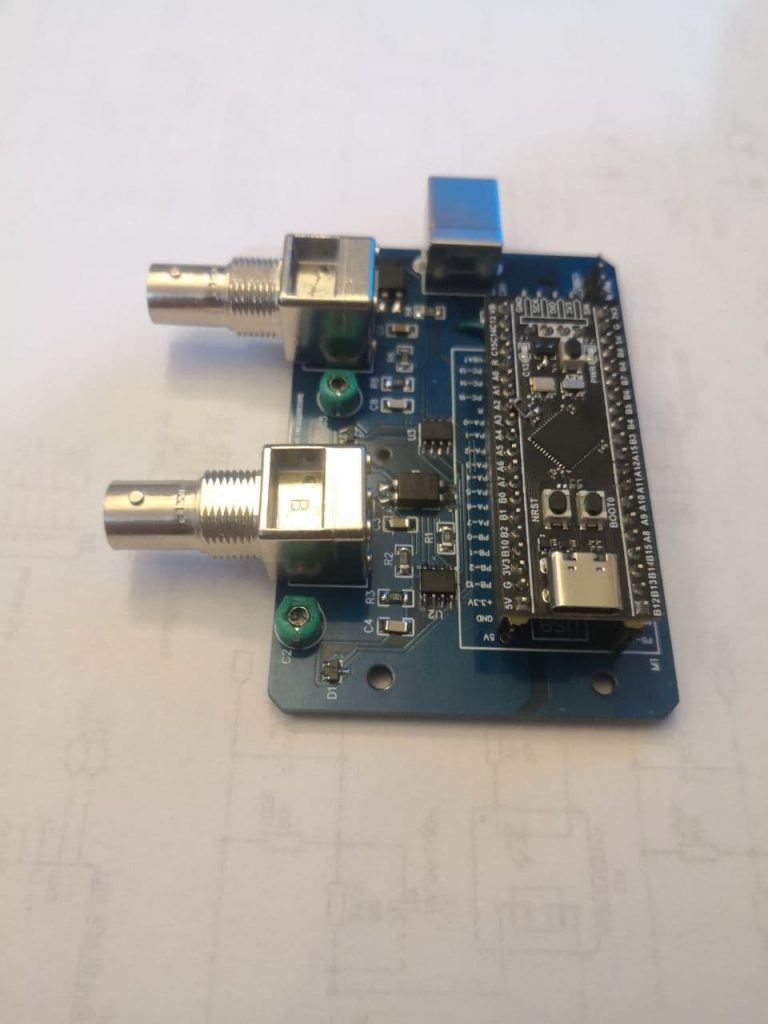
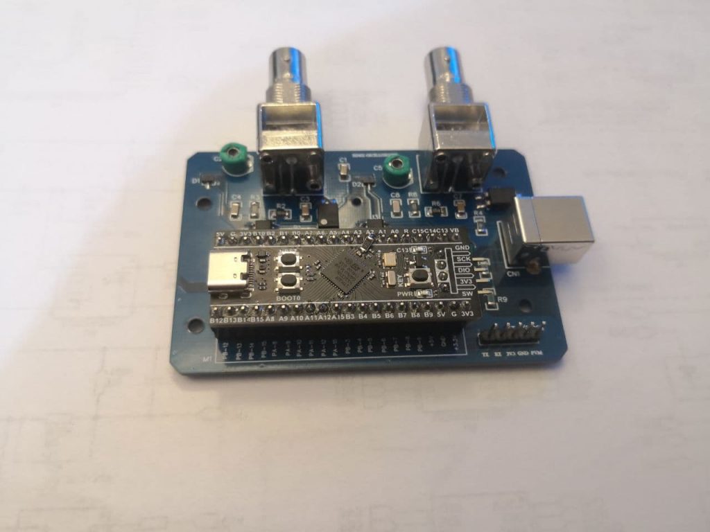
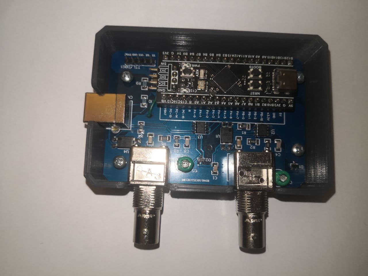
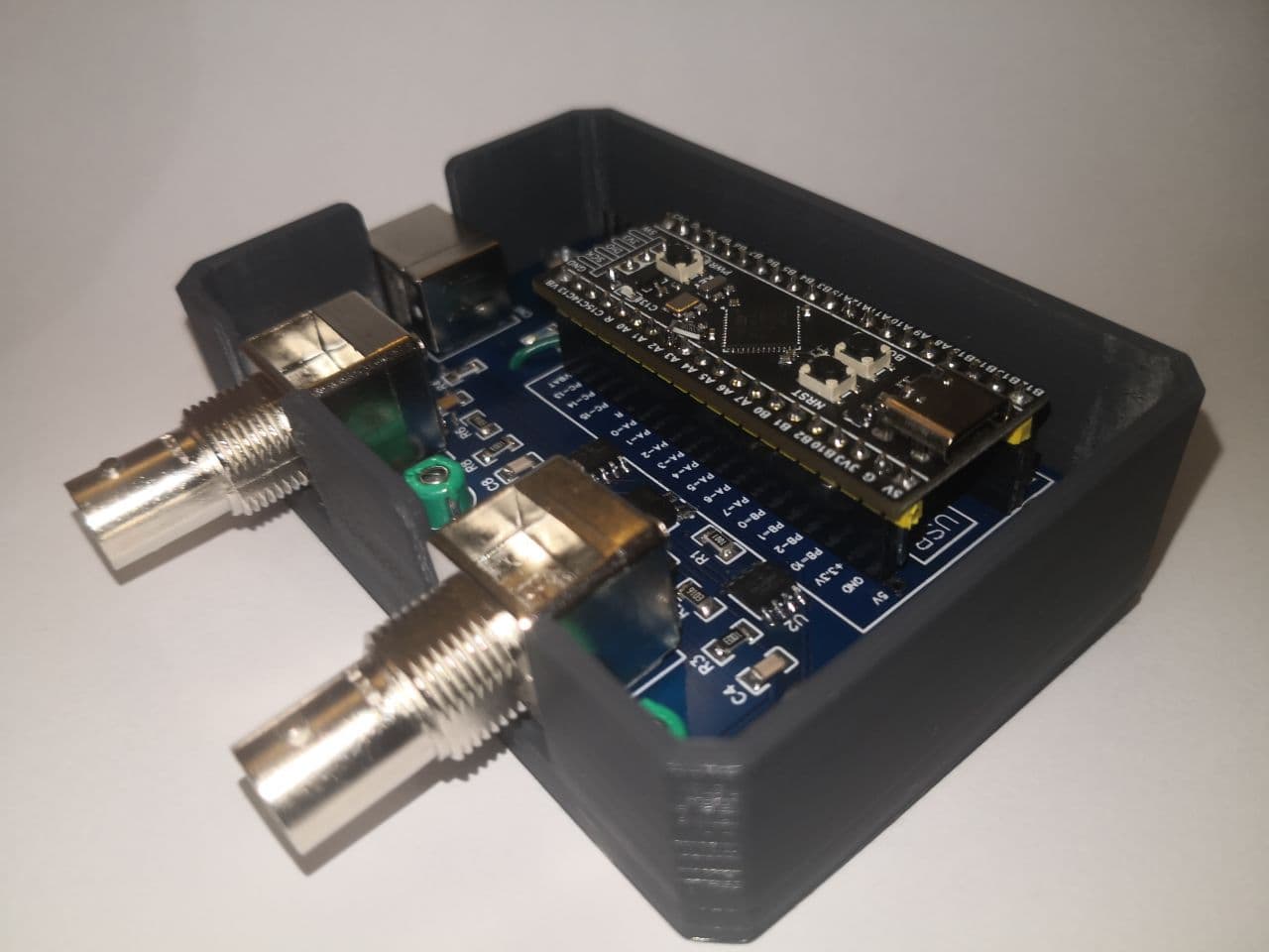
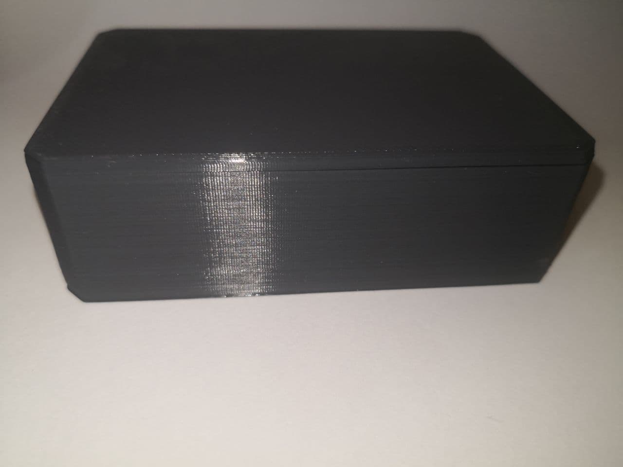
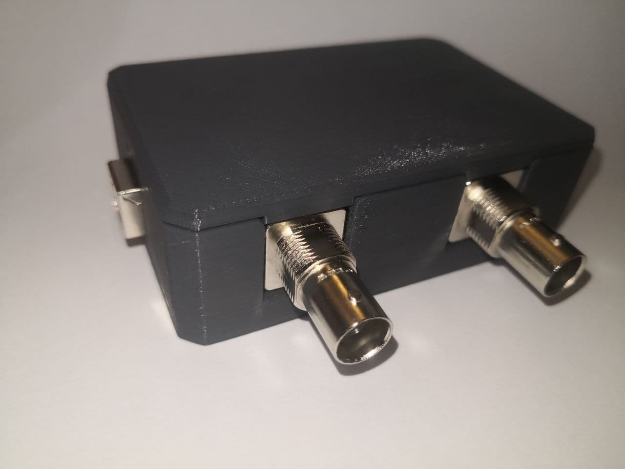
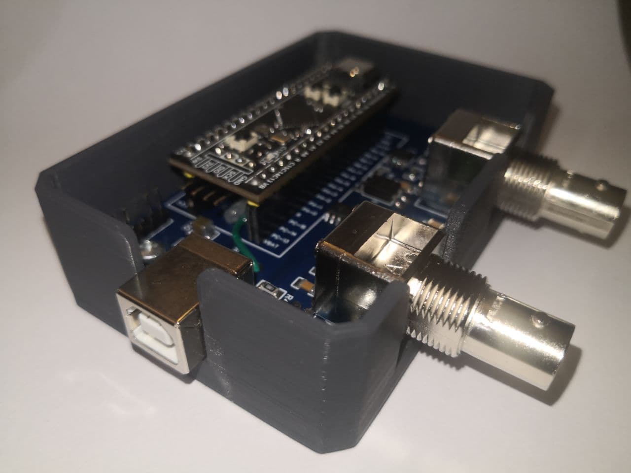
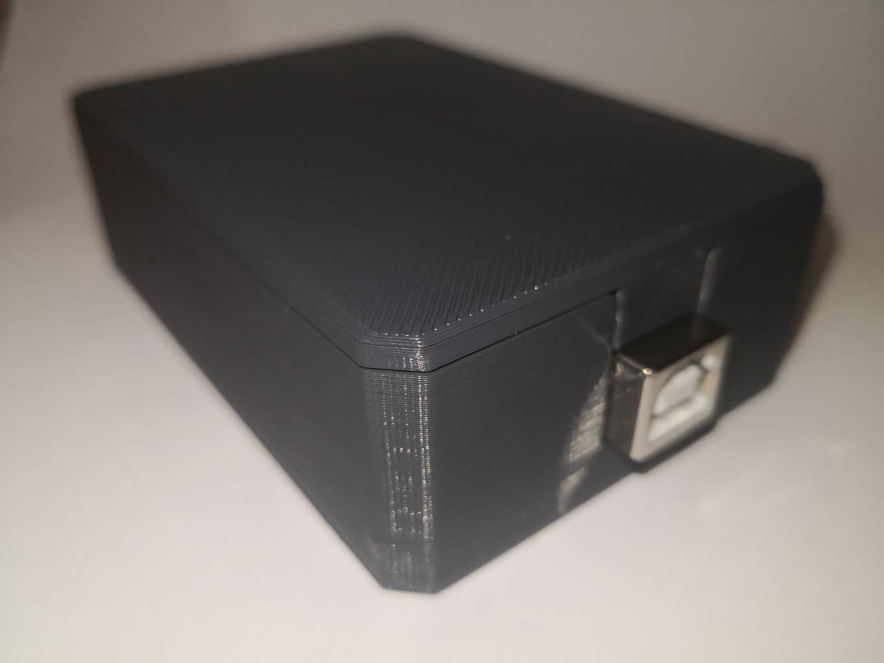
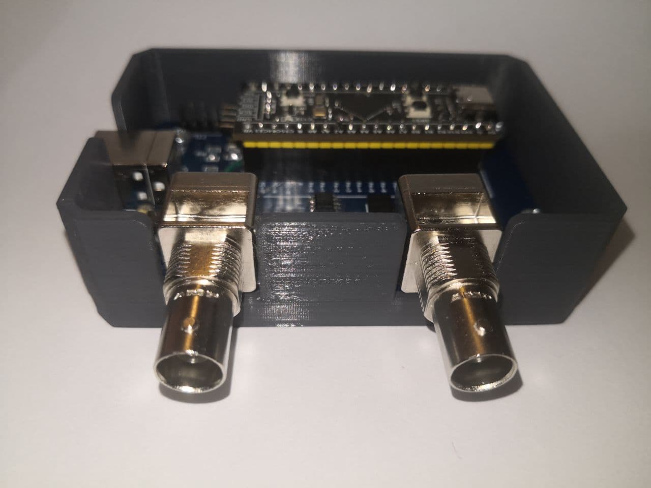
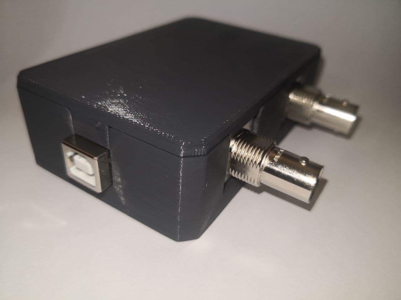
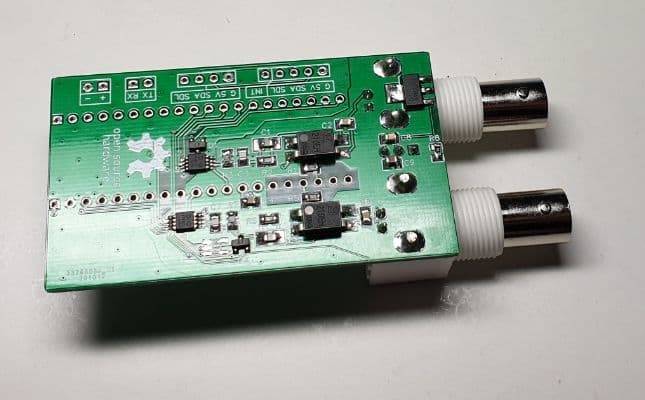
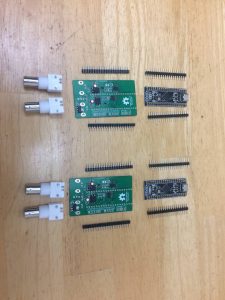
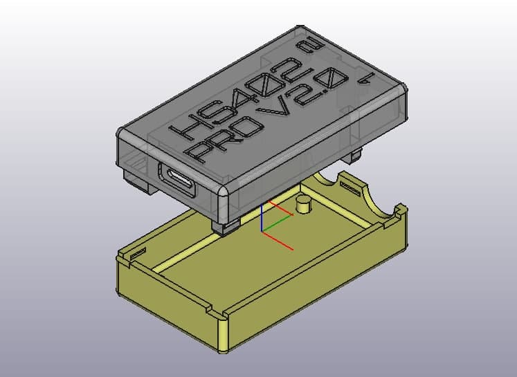
2. Full Built (with PCB v3)
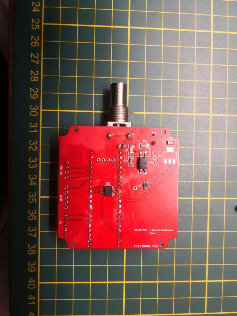
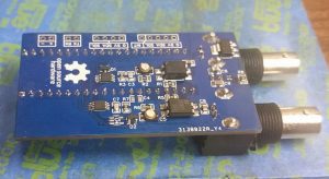
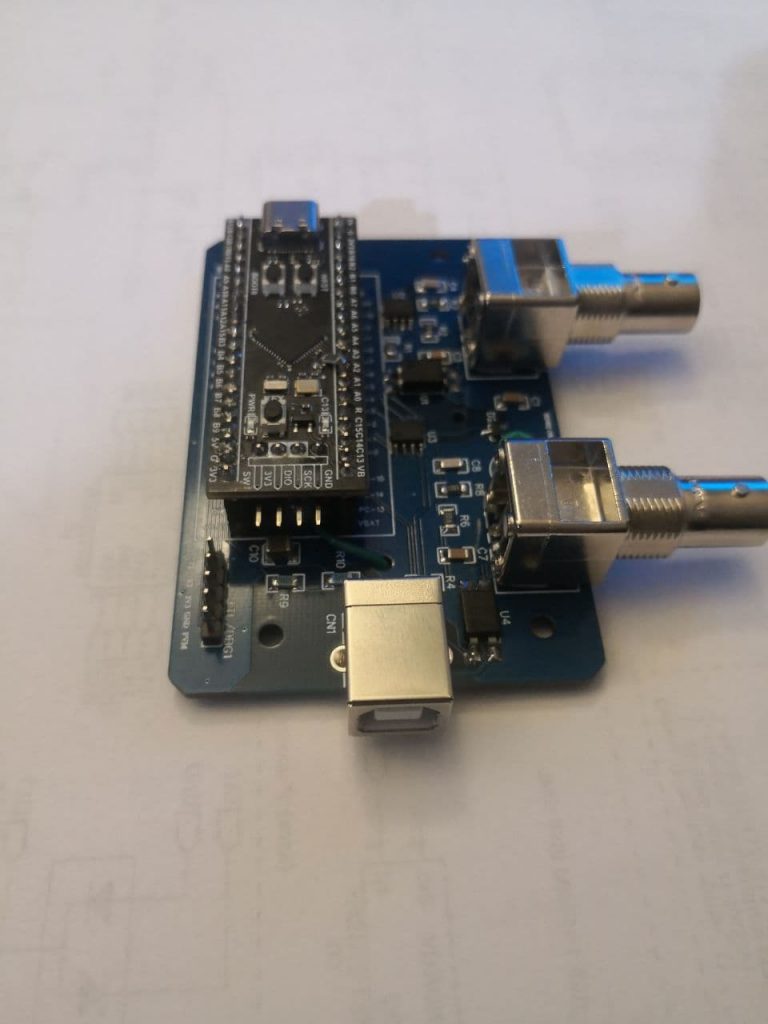
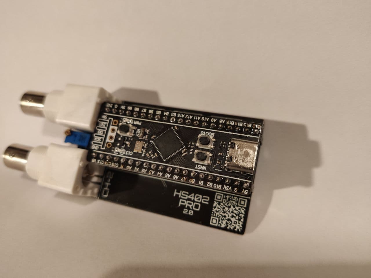
A compact built using PCB v3 which integrate all the components, including the ESP32-WROOM chip
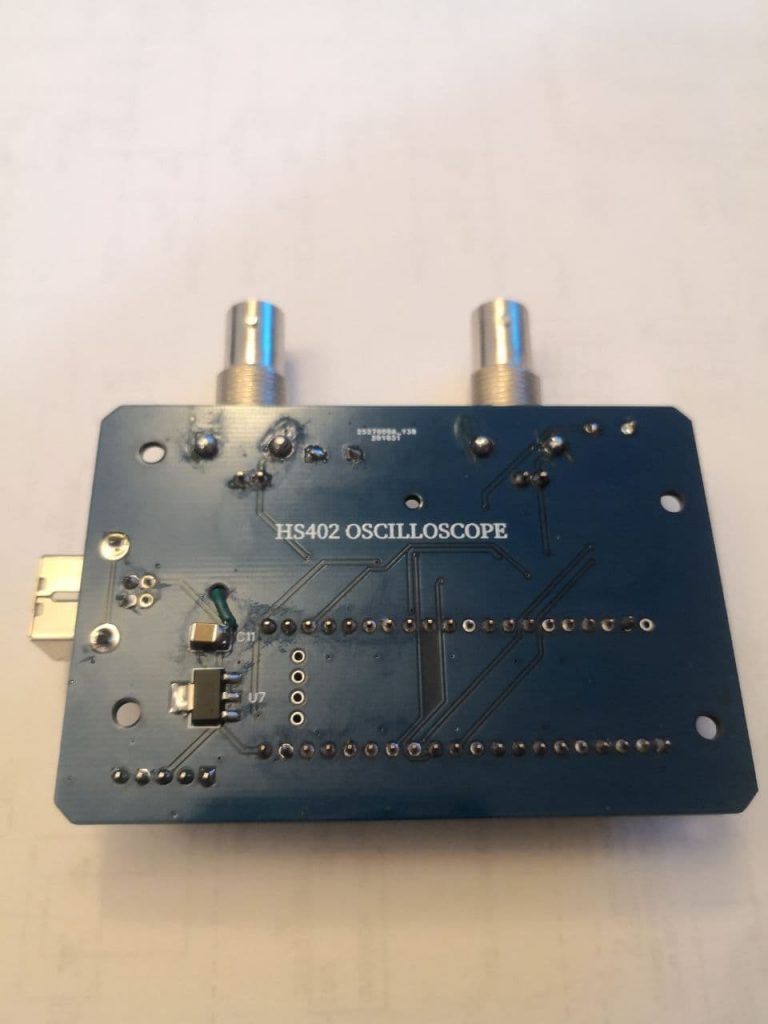
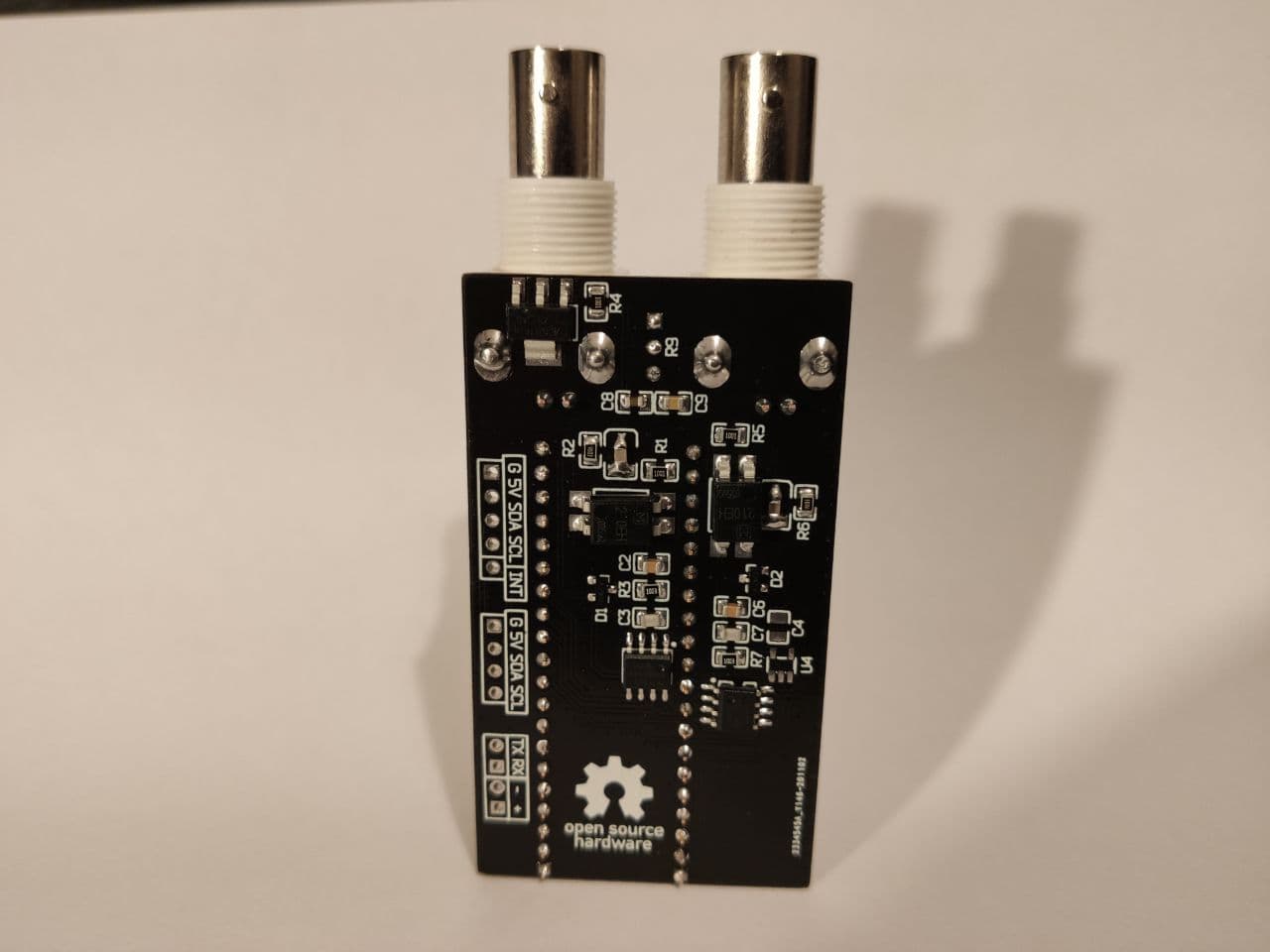
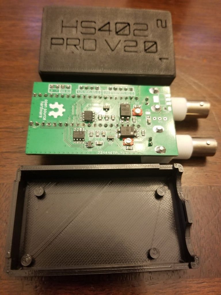
PCB v3 is composed by 2 parts that need to be separated. Then main PCB is for the standard HS402 USB oscilloscope, the small PCB is the WiFi Module.
You need:
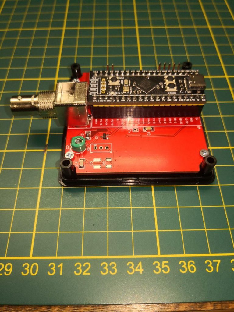
Get PCB v3, split the 2 board along the separation line by using a knife on both side and the apply a pression on both side to take the 2 board apart.
Solder all the components. A demo of the STM installation for PCB v3 is here.
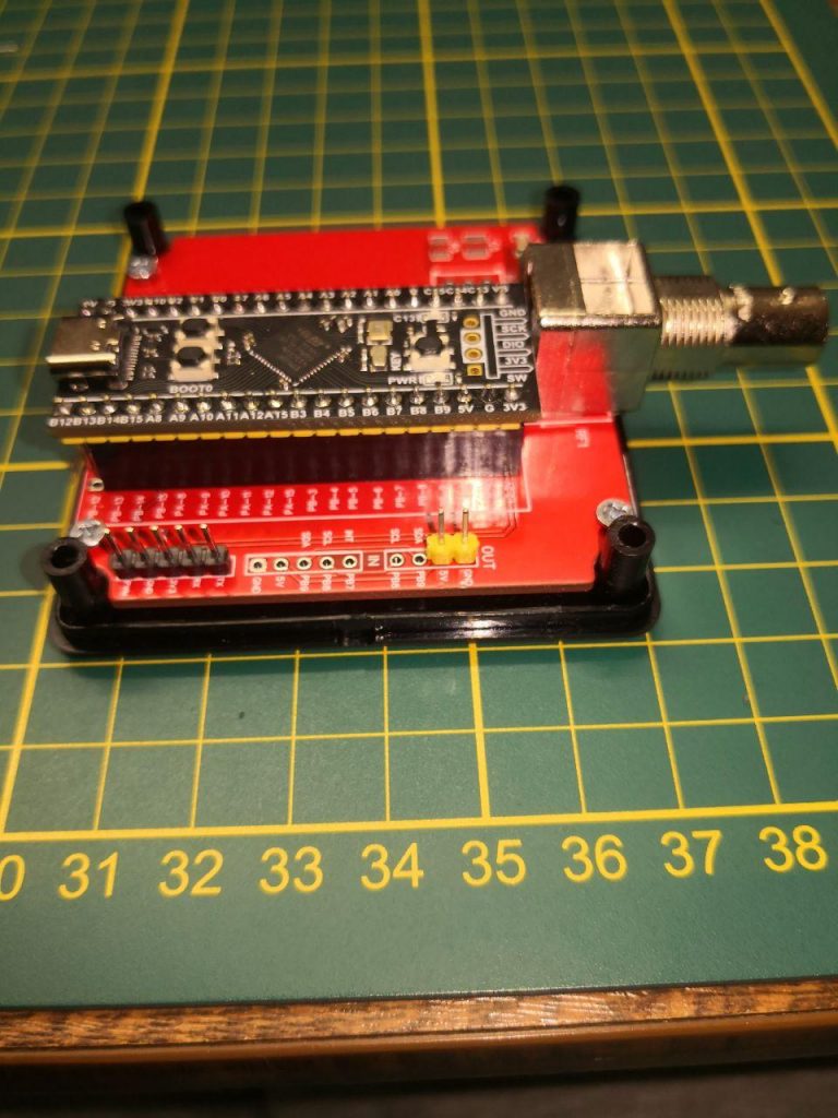
Flash the STM32 and the ESP32
Put the WiFi Module over the HS402 long connector (top right)
Power from BAT connector (3.6 – 5V) or from USB connector of the STM32
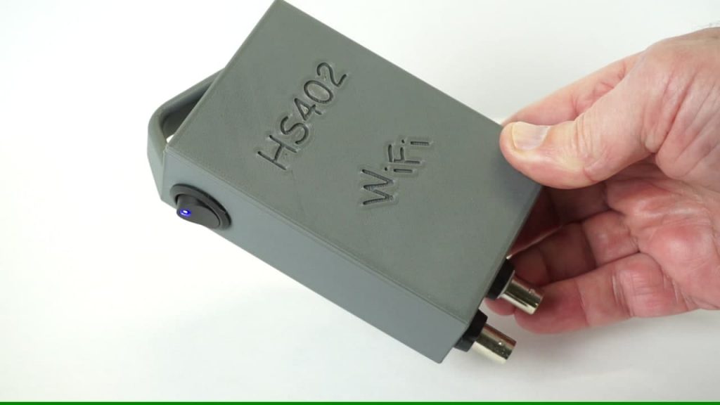
After just follow the User Guide to connect the WiFi configuration page.
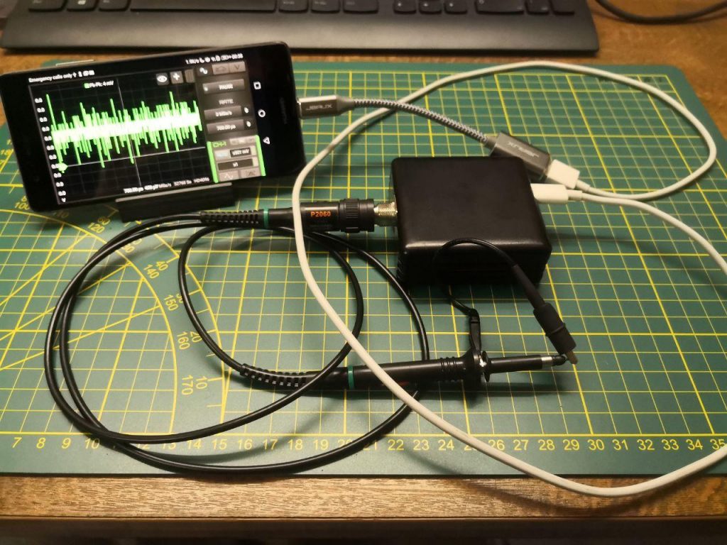
Just connect a classic phone charger to the USB port of ESP32 or of the STM32 to power up the oscilloscope. You can also disassemble a phone charger and add a switch for power, as done in this video.
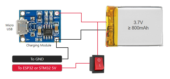
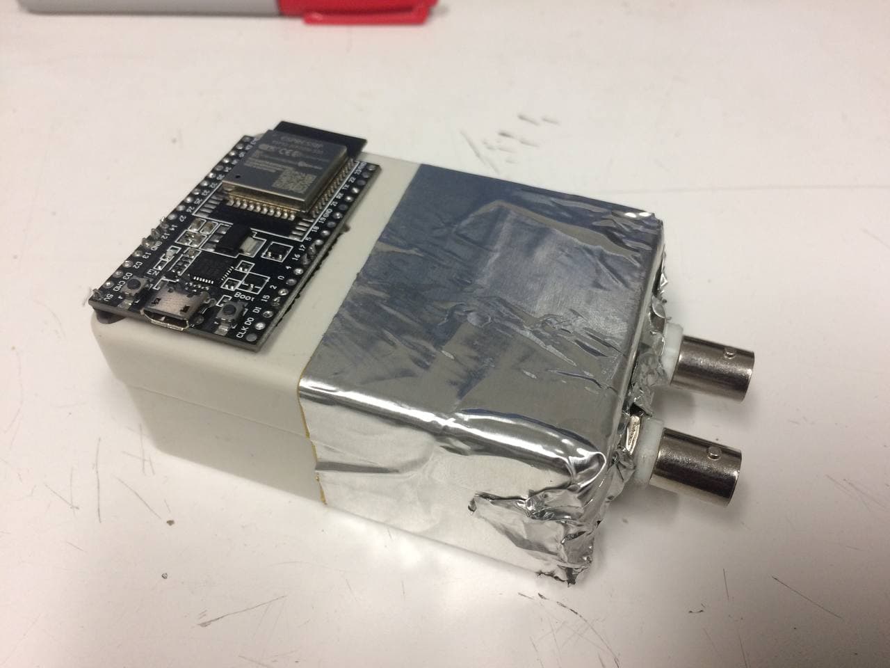
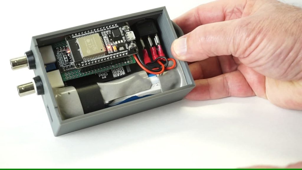
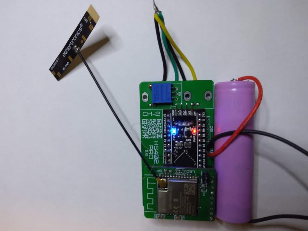
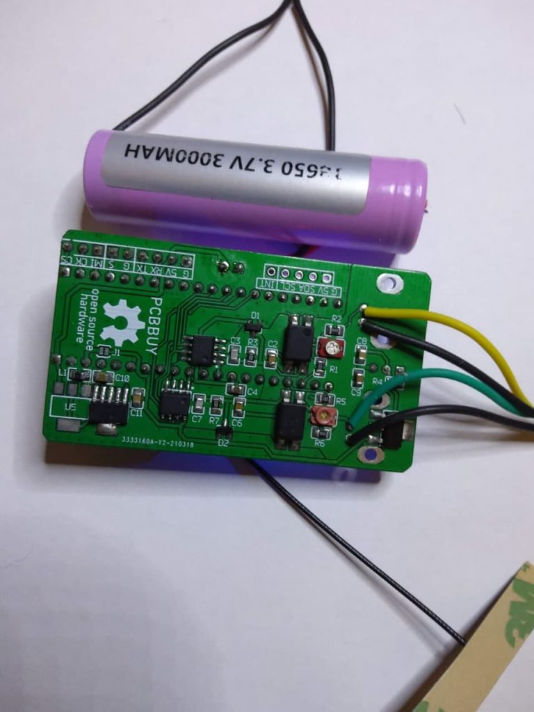
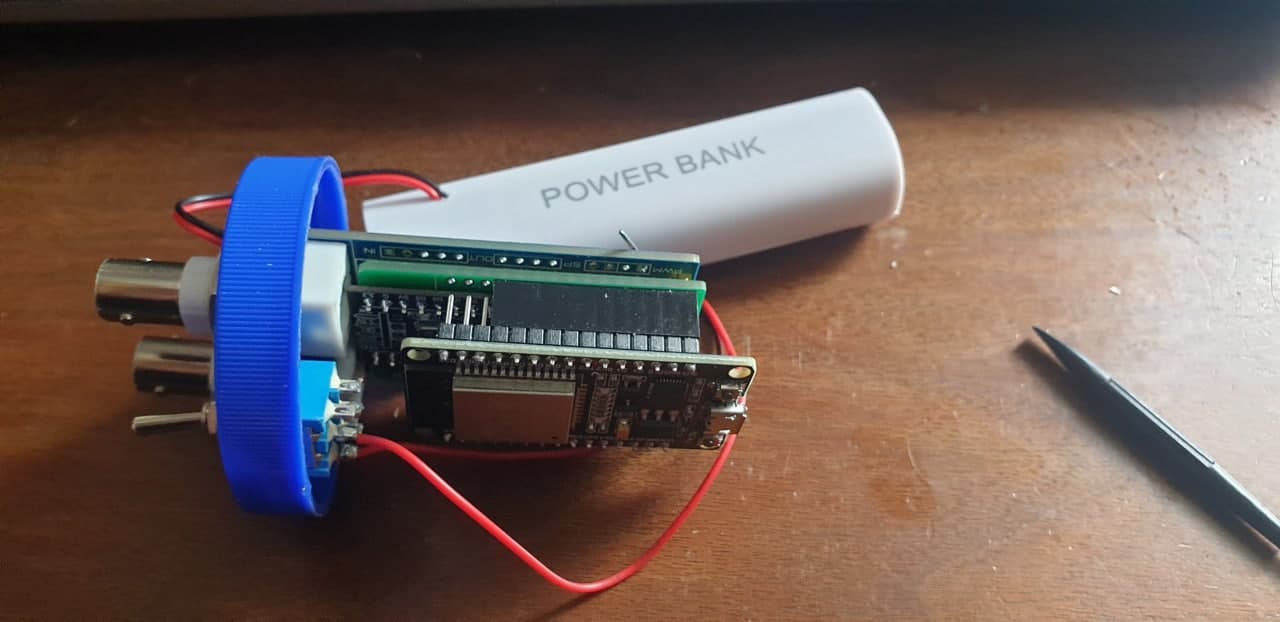
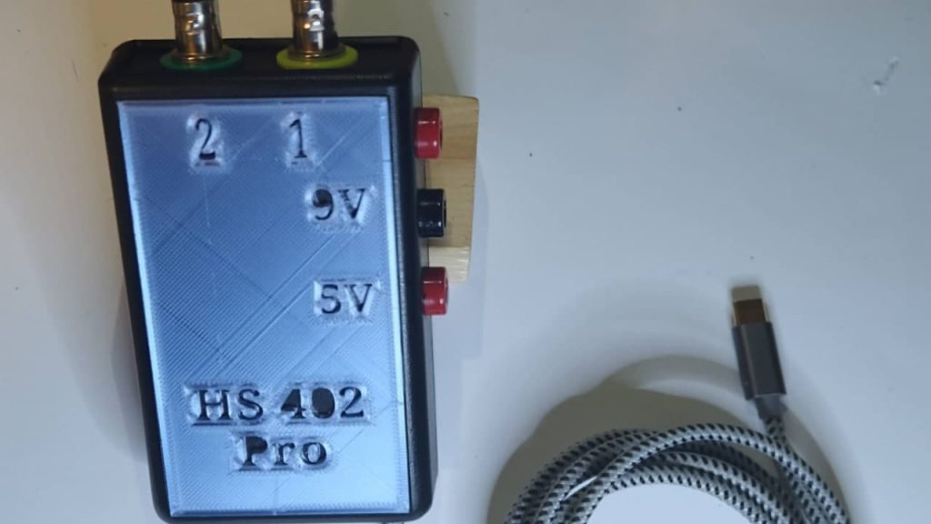
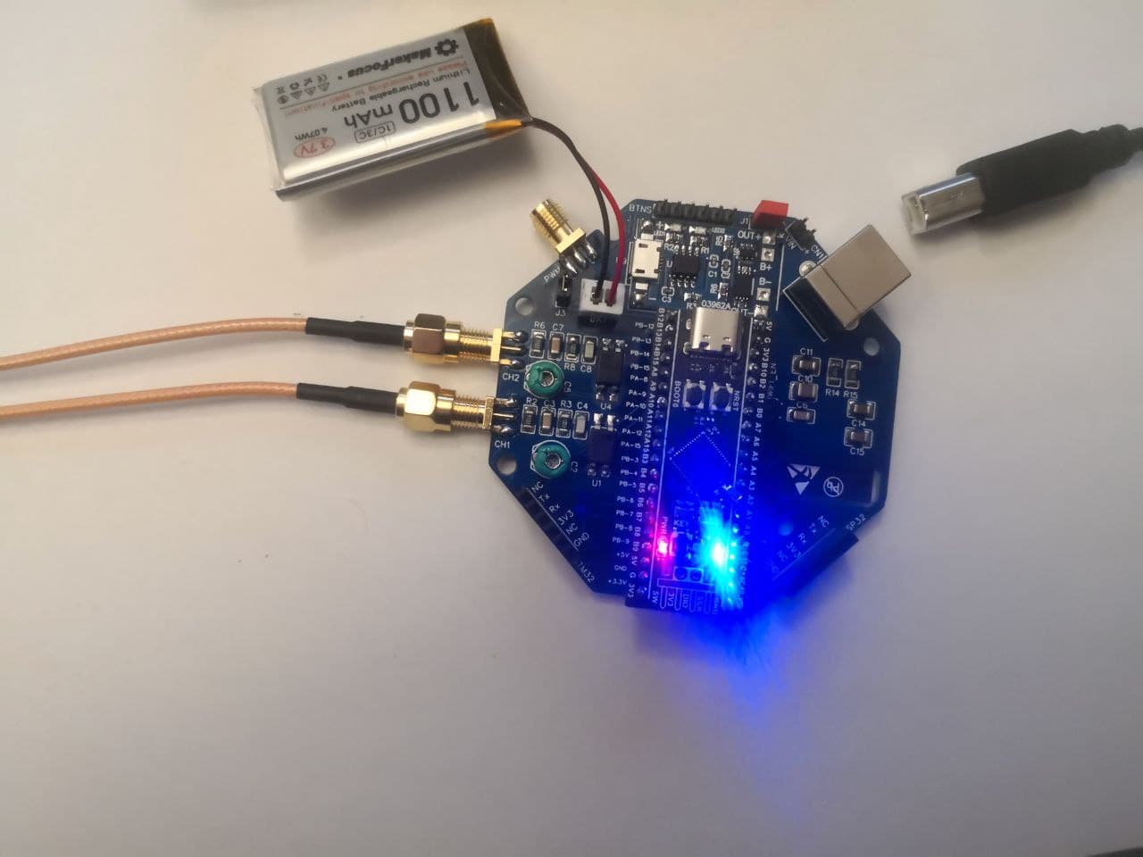
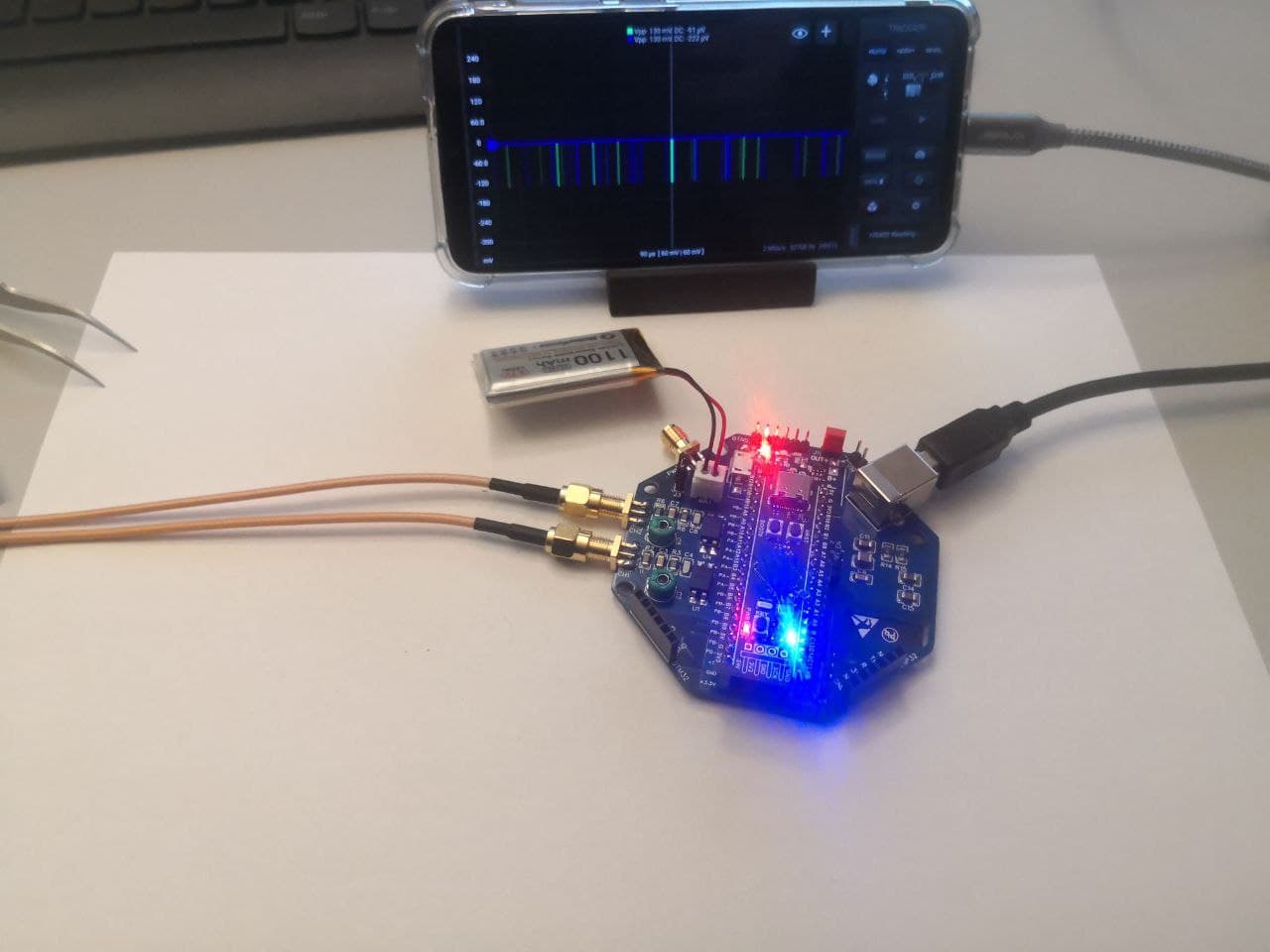
2. With 3.7V Lithium Battery
Possible only by using the hardware Option 3 in the PCB v3
With the hardware Option 3 in the PCB v3 it is possible to power the oscilloscope directly with a 3.7V Lithium battery. You can add also a micro-charger circuit as in the following schematic. This configuration allow the lower power consumption for this device (around 180mA avg).
Resources
Open Source Hardware Schematic for HS402-WiFi V3.0 available here.
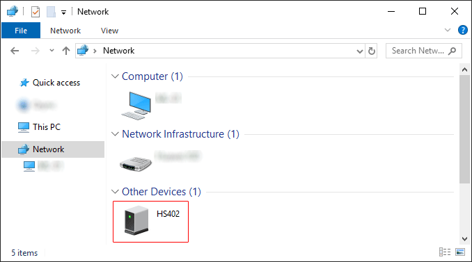
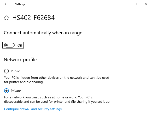
At the first boot the HS402-WIFI oscilloscope creates an Wifi access point with SSID like HS402-F62684. Connect to it with the phone or PC (password: 123456789) and open the browser (everything except Internet Explorer) at address 192.168.4.1, to access the oscilloscope configurations.
In windows you can find it also under Network. Double click on the icon to open the configuration page.
In case you cannot see the oscilloscope in the Network list, in the wifi list just open the preferences of the HS402 wifi and set it as Private since Windows block the device discovery on public networks.
Oscilloscope Configurations
Network
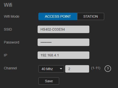
The oscilloscope can work in one of these modes:
Access Point (or AP): the oscilloscope become an access point and the phone can connect to it directly by using its SSID name (for example HS402-F62684). You can configure SSID name, password, IP and WiFi channel. 40Mhz WiFi channel is faster and generally suggested. For the WiFi channel selection it is suggested to run a WiFi scanner to check which channel is more free in your area.
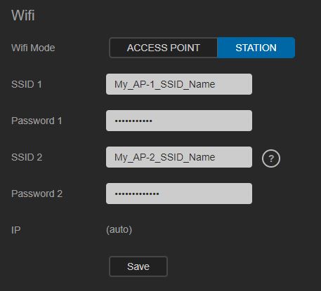
Station (or STA): the oscilloscope connect to an existing access point (for example a residential one) and can be found by HScope in the same network.
You can set 2 different SSID, the oscilloscope will try to connect to the first one, in case of failure it will try the second one, in case not possible the oscilloscope will turn to be Access Point using the access point settings.
Remember to reboot the ESP32 (or press the reset button) to apply the new WiFi settings.
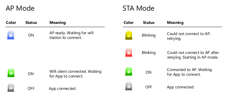
LED Messages
The RGB led connected to the ESP32 development board provides the status of the oscilloscope.
AP Mode: the ESP32 is itself an access point, you can connect to it directly by searching on the available Wi-Fi. SSID like HS402-F62684. STA Mode (Station Mode): the ESP32 connect to an existing access point / router. The phone / tablet should be connected to the same network to connect to the oscilloscope. You can configure this mode in the ESP32 Webpage.
HScope Configuration
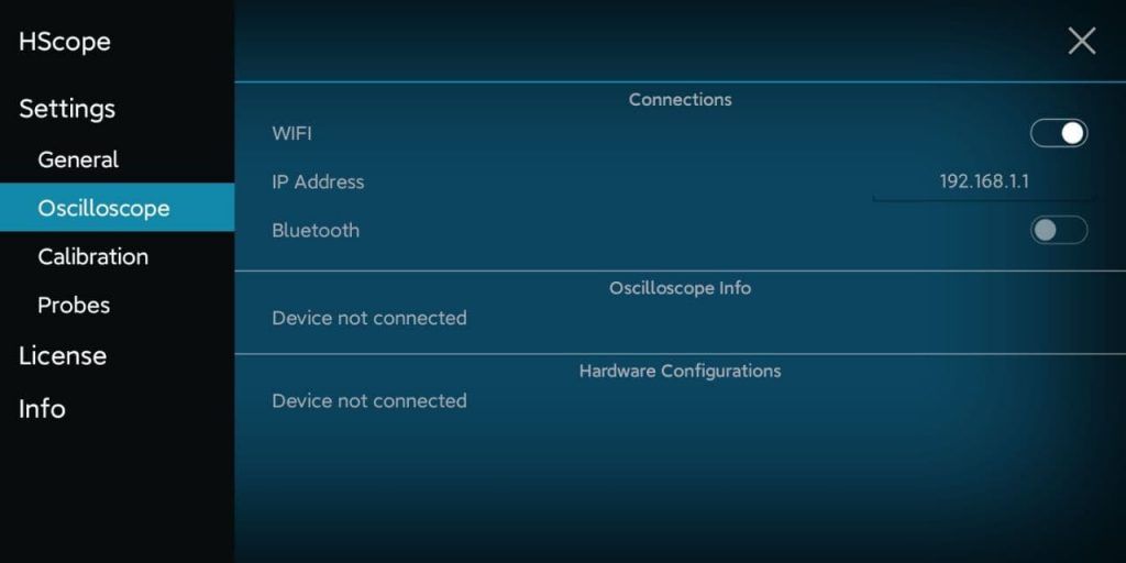
In HScope you need to enable the WiFi connection. This setting in available in the Oscilloscope section:
Configuration Reset
In case you forgot the password of the Wifi in AP mode and cannot access the configuration anymore, just press the BOOT button to reset the configuration to the standard values.
Press and keep pressed the BOOT button for at least 3 seconds. The LED will blink in yellow color.
Release the button, then the LED will blink in red color to indicate the configuration update and the ESP32 will restart automatically in AP mode with the default SSID name and password.
Possible Issues
The app disconnect from the oscilloscope after a while
This may be due to the Android phone/tablet that disable automatically from the ESP32 network and connect to another network. To avoid this you need to disable in the Android settings the automatic connection to stronger networks.
Remove WiFi automatic connection to strong network in Android. In this way the oscilloscope won’t disconnect if the Android tablet detect a stronger WiFi connection.
The app disconnect and reconnect
This case has been found from some user and it is related to the fact that the phone/tablet run other processes using the networking and slowing down the connection with the oscilloscope which goes in timeout and then reconnect. This has been solved by deactivating the Bluetooth in the Android tablet/phone (enabled Bluetooth used to run frequent scans blocking the WiFi communication).
If you want to have your project published just drop an email!
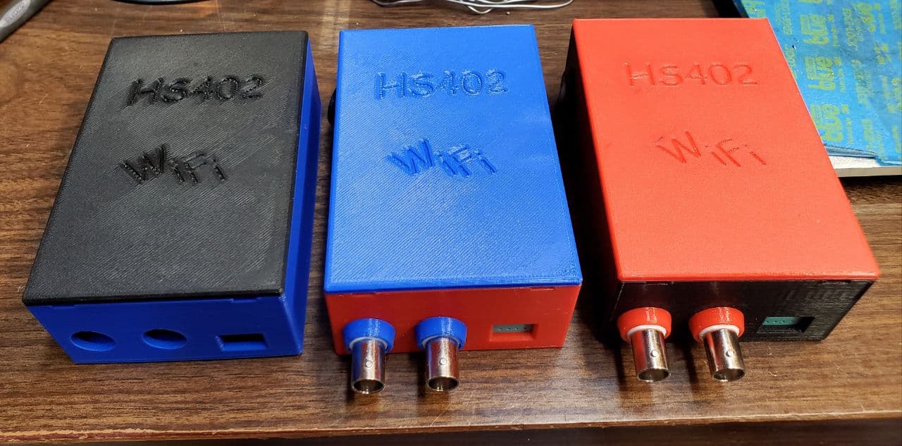
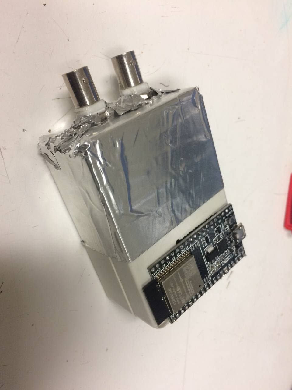
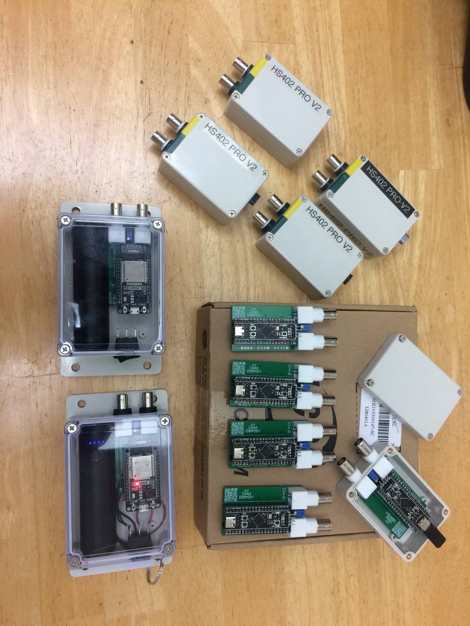
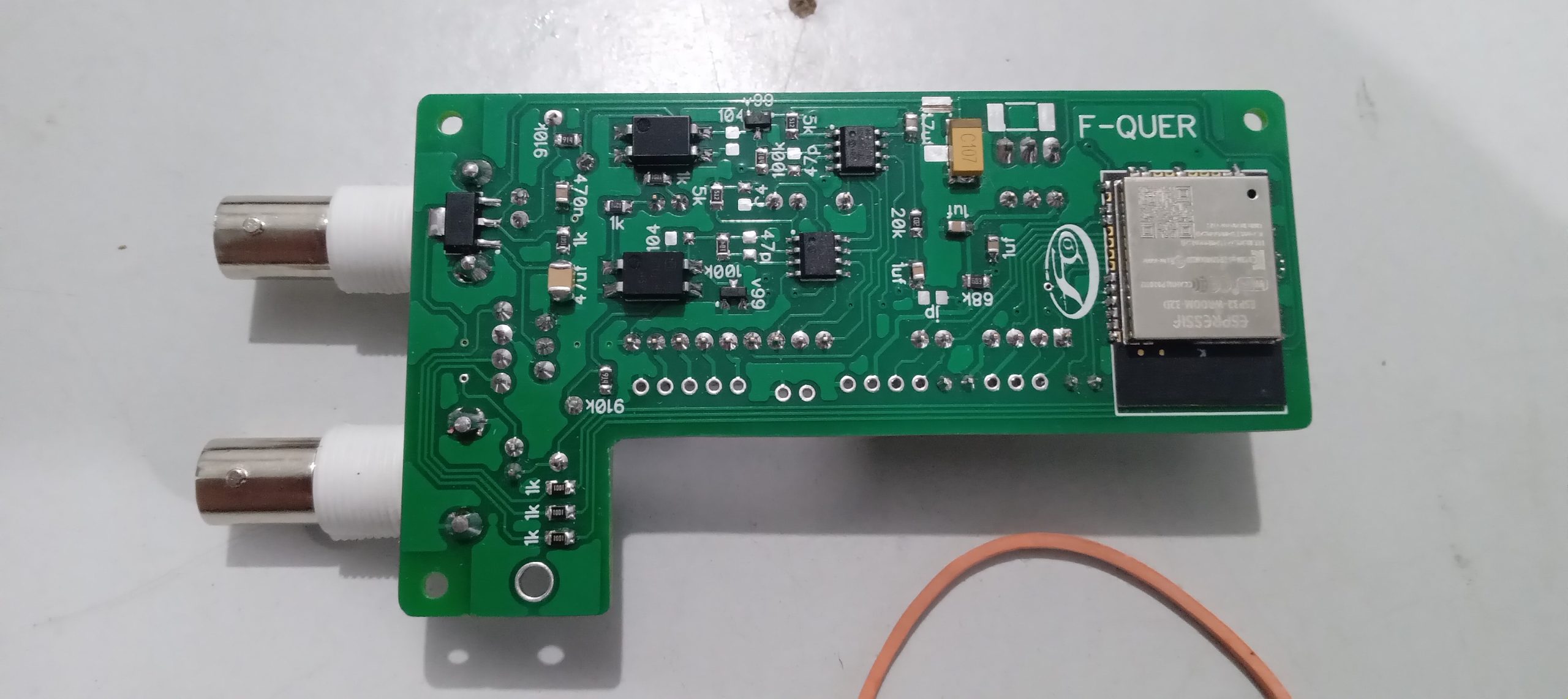
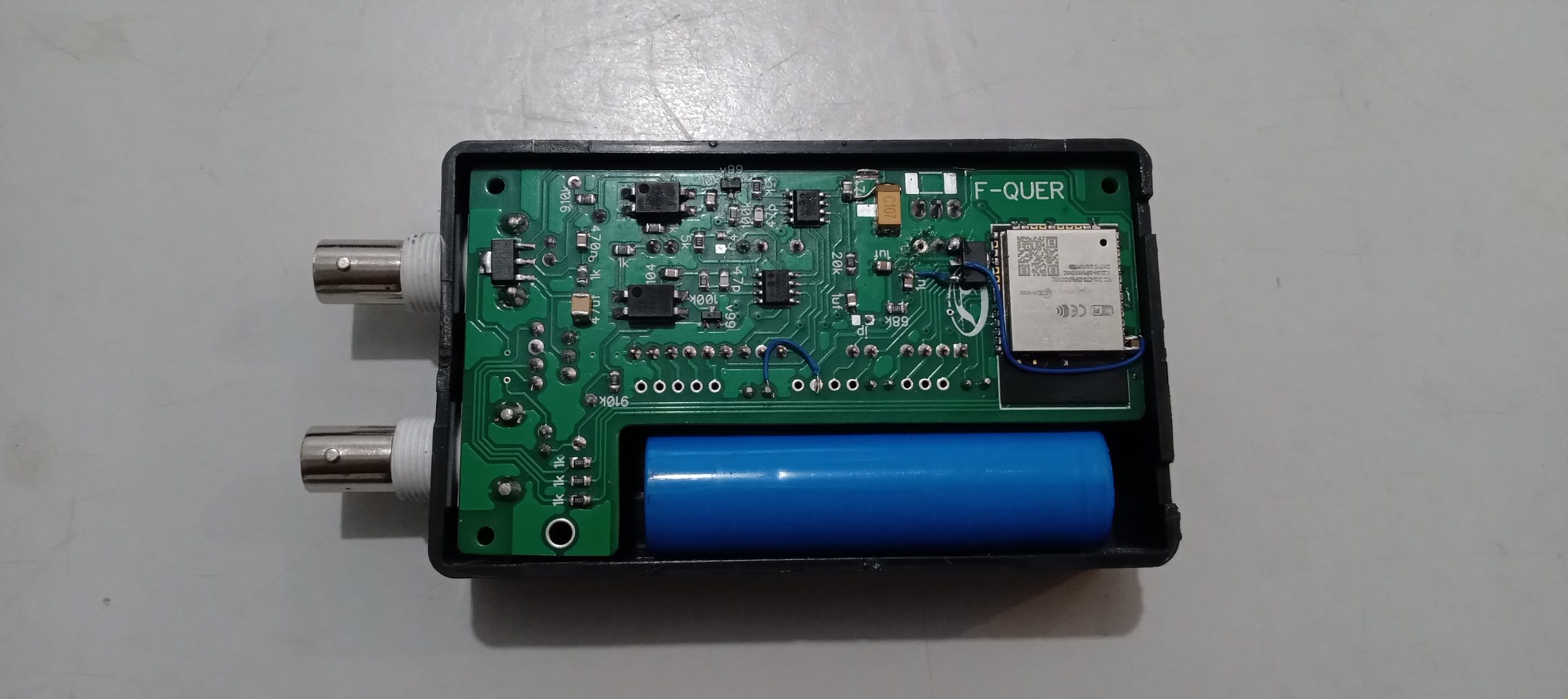
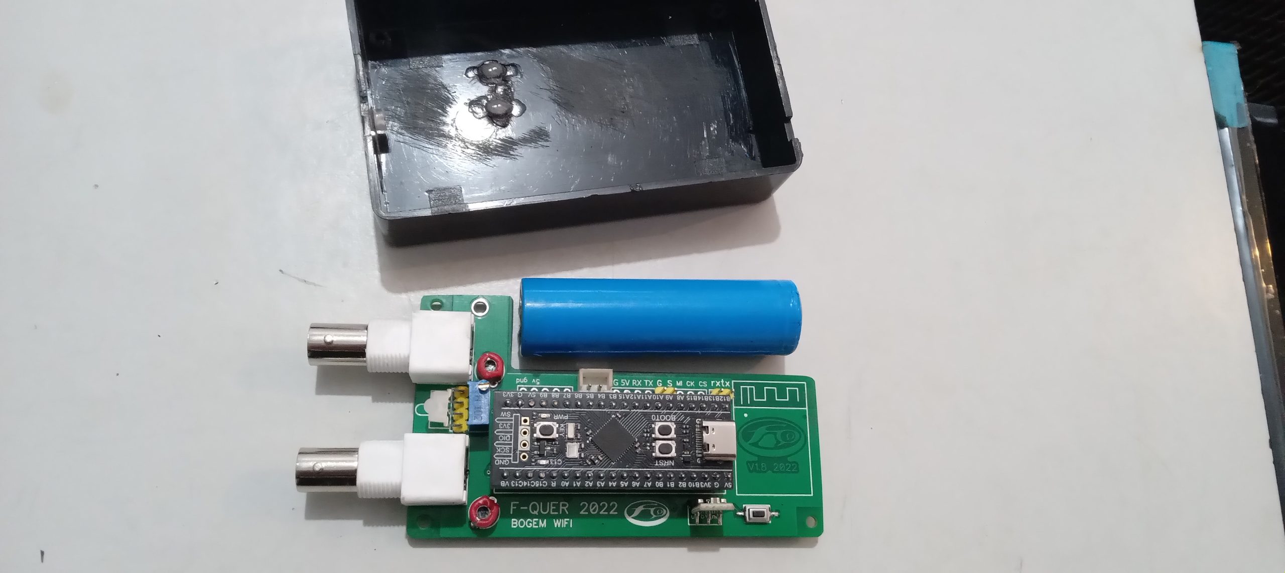
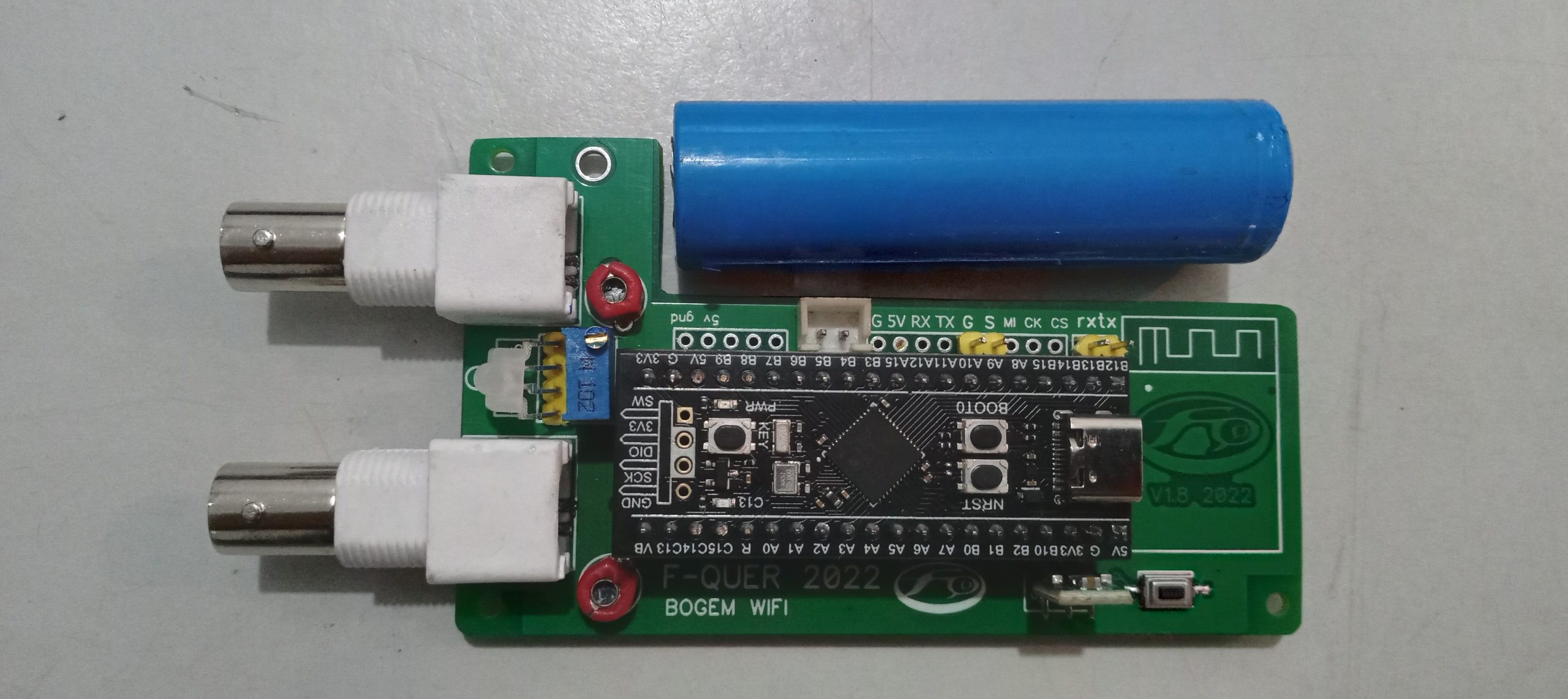
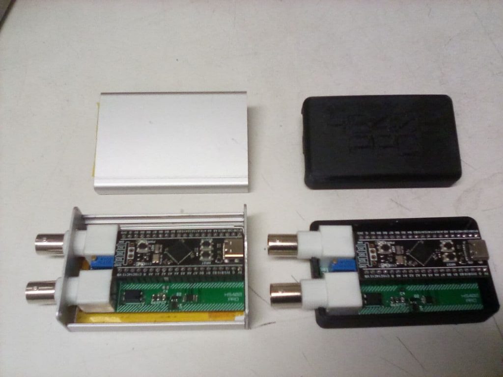
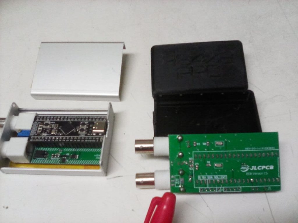
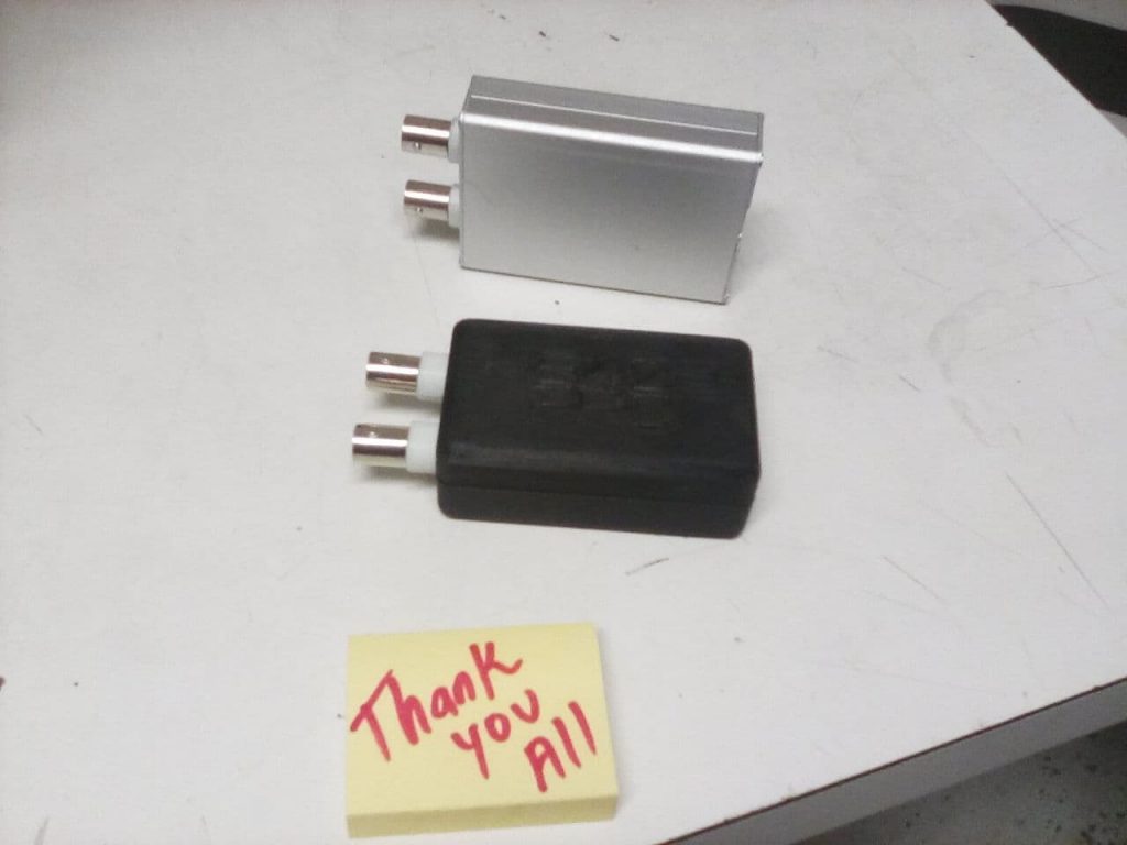
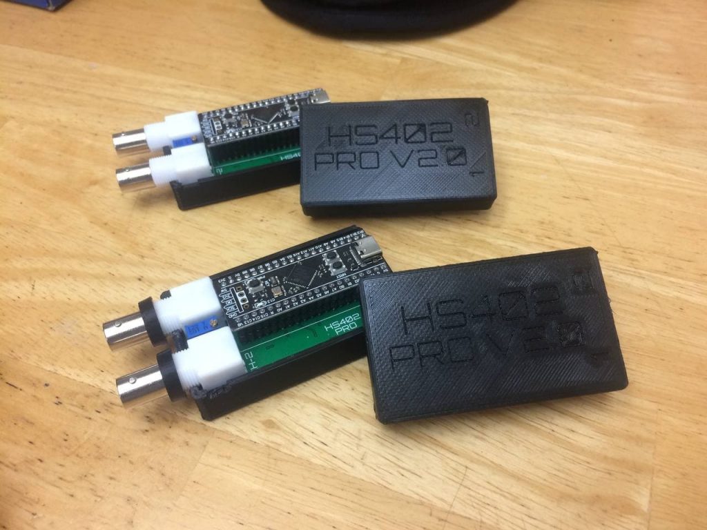
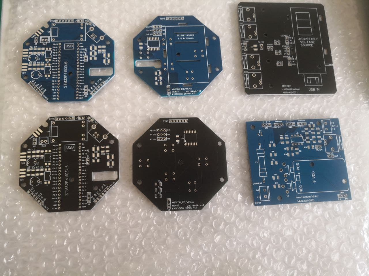
Built by Mikael (2021)
Built by Chris (2021)Built by Ramon (2021, using ESP32-WROOM-32D development board)Built by Denis (2021, using ESP32-WROOM-32 development board)Built by Jamie (2021)Built by Jim J (2021)Built by Trou B (2021)Custom PCB by F-QUER
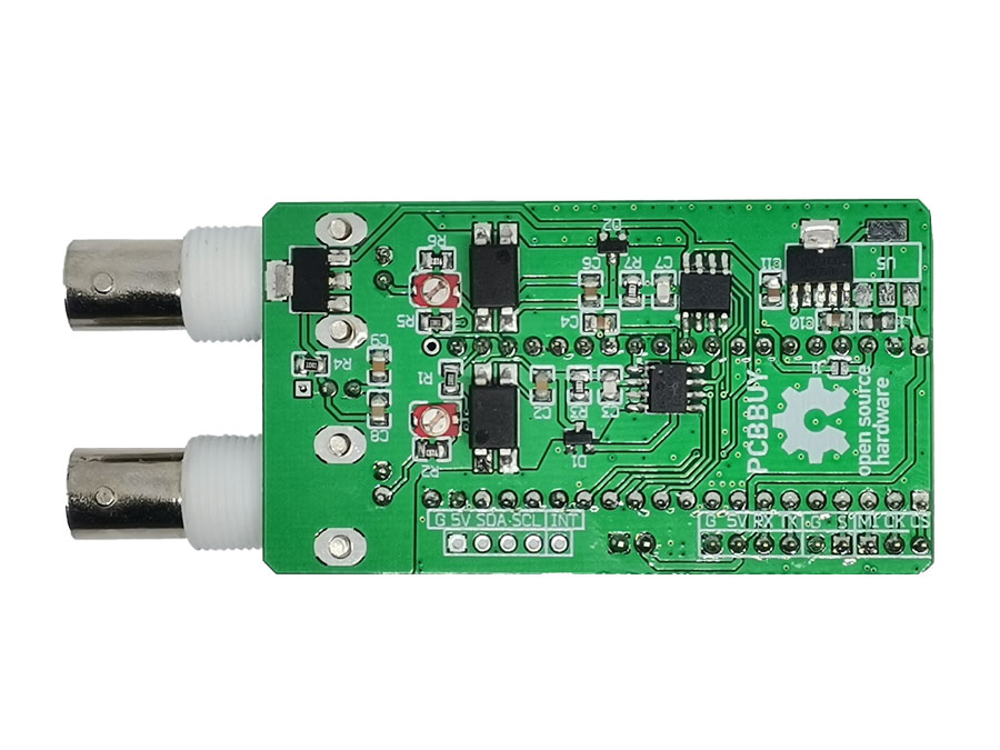
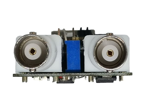
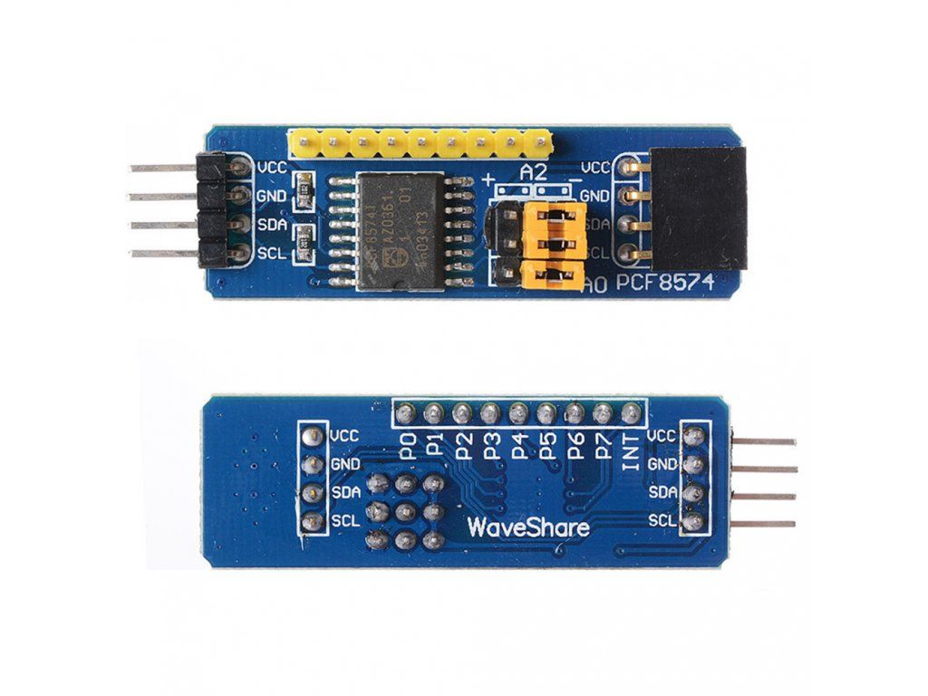
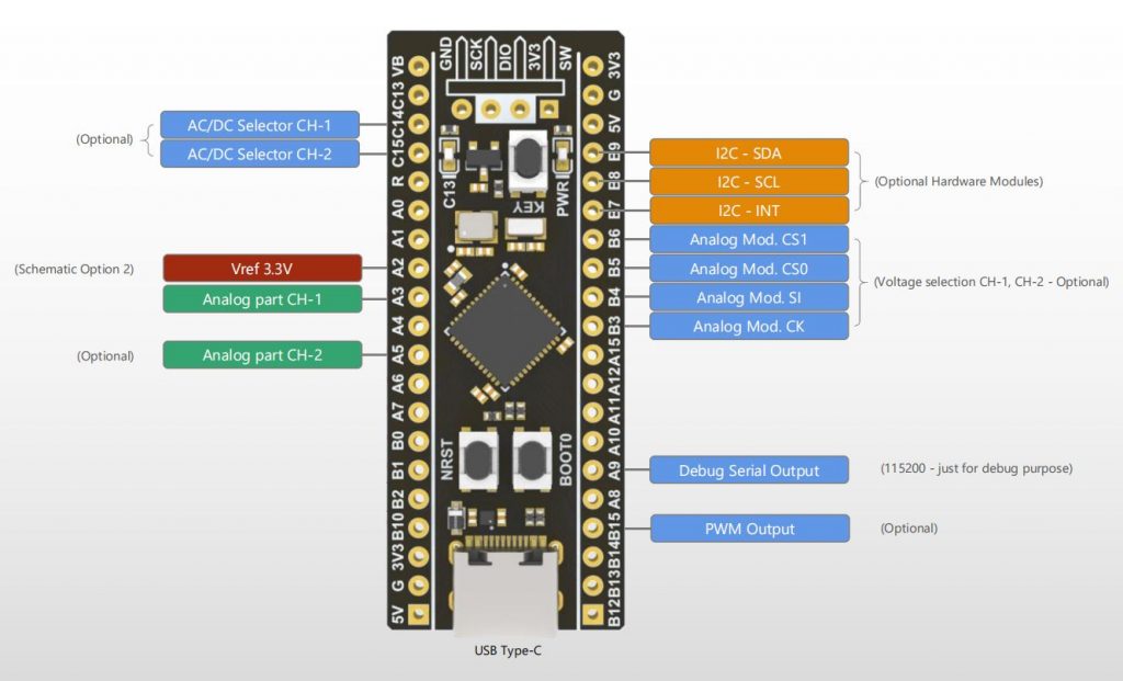
By connecting the PCF8574 I2C module it is possible to have 8 hardware buttons to control the oscilloscope. These are the pin that should be connected to the STM32: GND, VCC (5V), SDA, SCL, INT. Buttons are triggered by connecting the P0-P7 pins to GND. The configuration jumpers on the PCF module should be as in the picture (it use the base address).
Button functions
P0: Start / Stop
P1: Rate up
P2: Rate down
P3: Fit waveform to screen
P4-P7: (not assigned)
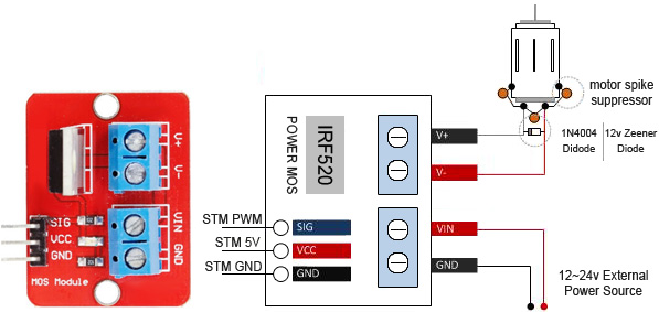
PWM Module
HS402 can generate PWM output. A MOS driver like the MOSFET IRF520 Module Board can be used to control loads. Here the schematic of connections. A video about how to use the HScope PWM module is shown under. The IRF520 has been tested at 1KHz PWM frequency and showed low pass characteristics so it is not suggested to use an higher frequency.
Other STM32F411 development boards can be used, the important is that the main crystal is 25MHz
On the schematic are indicated 2 or 3 hardware options. One exclude the other.
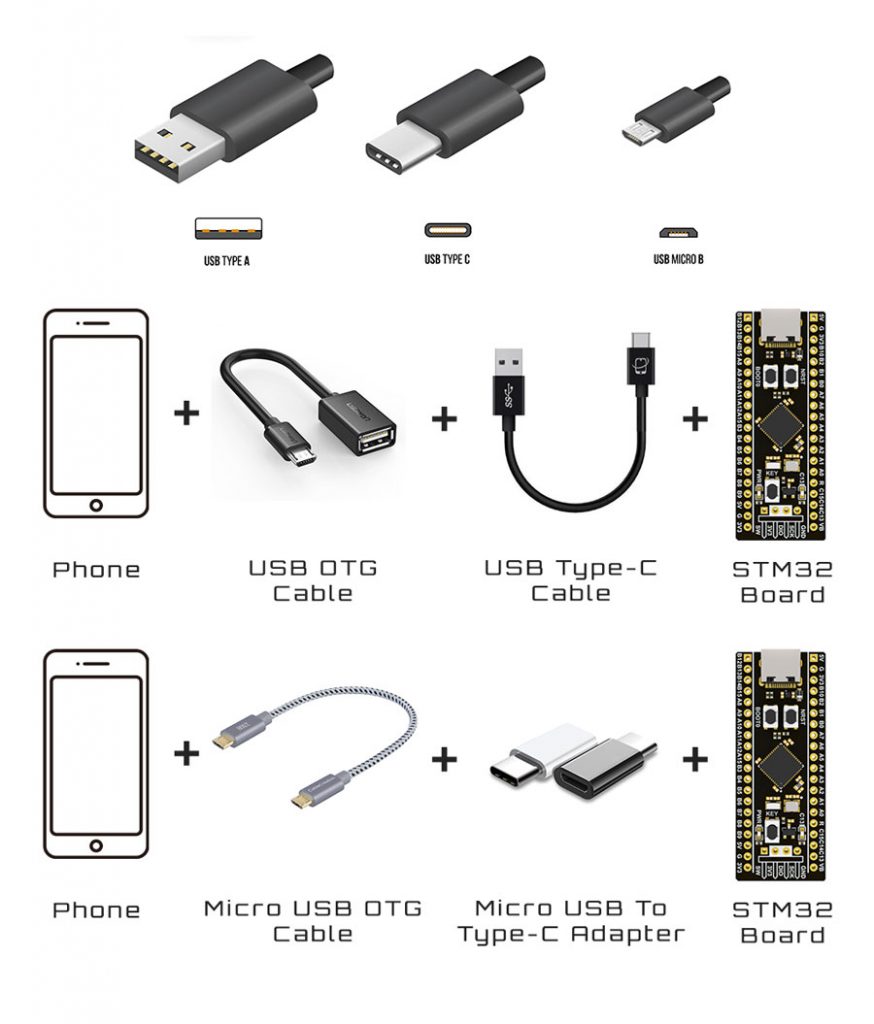
Flash the Firmware
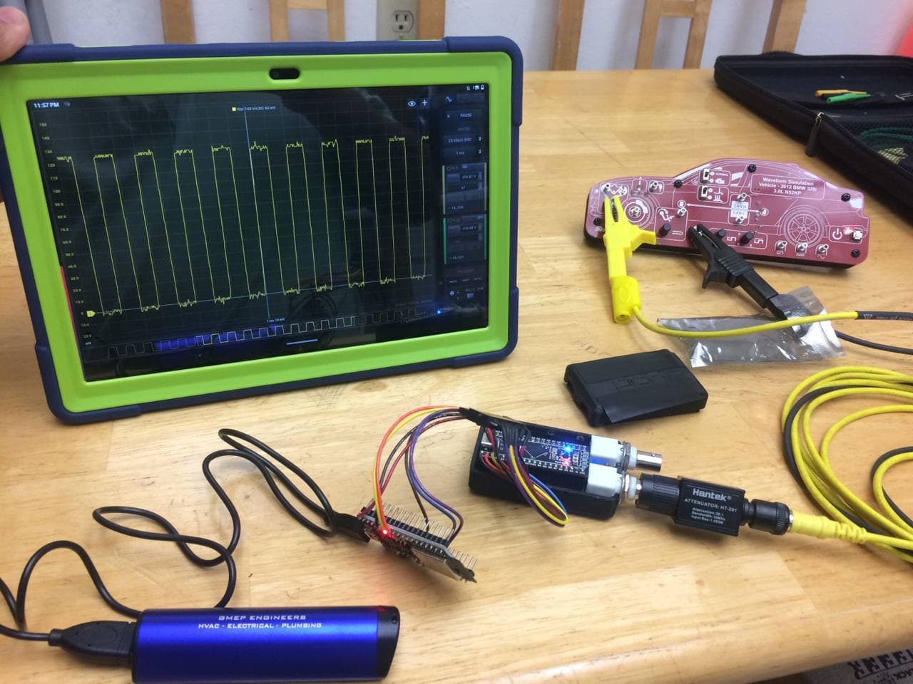
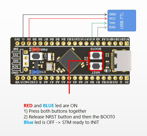
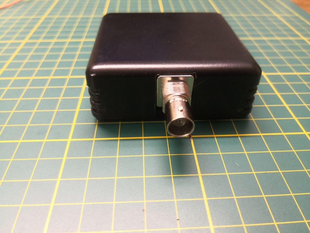
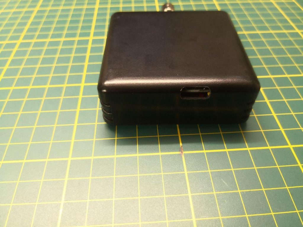
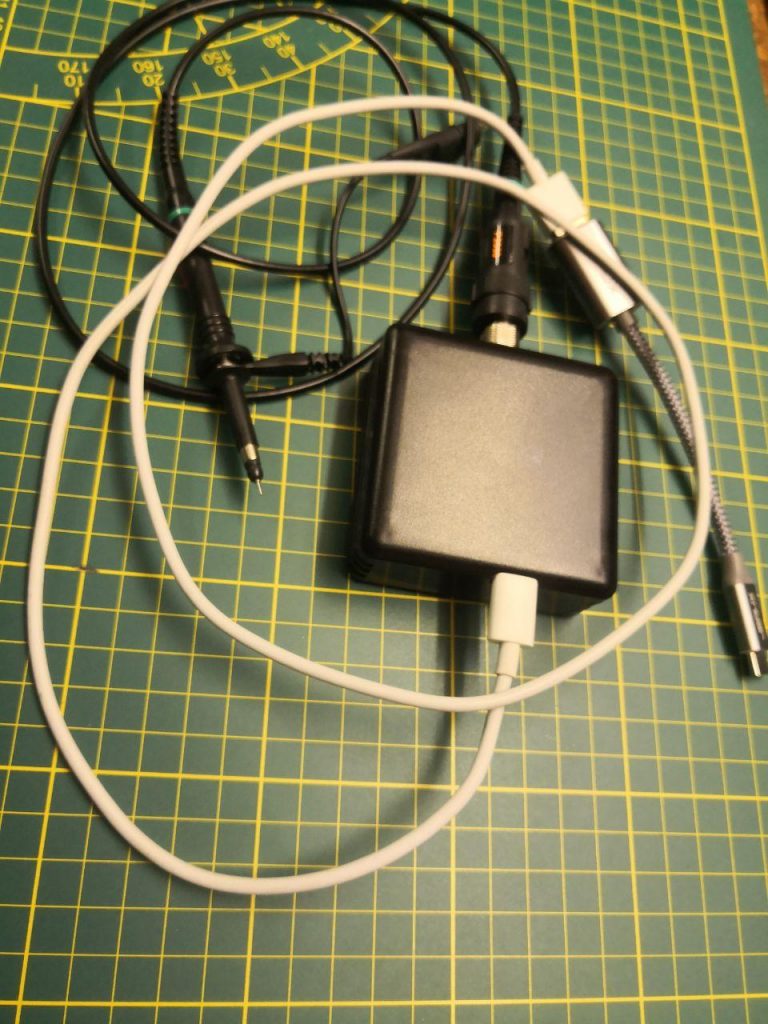
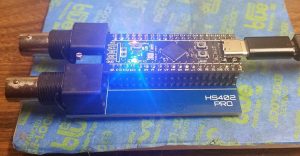
The firmware flashing is made with the app STM32 Utils with an OTG adapter connected to the phone and an USB-TLL adapter connected to the OTG adapter. After connecting the phone to the STM32 Black Pill board like in picture, the red led light up.
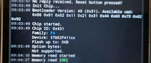
By pressing the buttons on the Black Pill as in picture, the board enter into the STM boot loader and it is ready to be flashed. On the App: 1) Go to Init Chipset and check that the app read the chipset
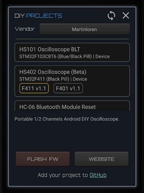
2) Go to the Blue Box icon and in the list under vendor Martinloren select HS402 Oscilloscope, select the chipset from the variants (STM32F411 or STM32F401), then FLASH FW.
3) After flashing disconnect the USB-TTL cable from the STM32 board and connect the STM32 to the phone through the OTG cable. Open HScope, the app should show you the signal from Channel 1.
Connection
First Setup / Calibration
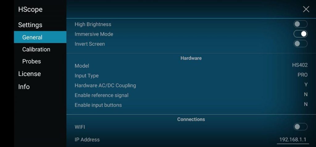
When the oscilloscope is connected go in HScope Settings, General - Hardware. Here:
Set the Model to HS402 and Input Type to PRO. When you do this change also the option Hardware AC/DC Coupling will be enabled automatically.
Disconnect and reconnect the oscilloscope to get the new configurations.
You can also Enable the input buttons if you have installed the corresponding I2C module.
Offset Calibration
(required just for Hardware Option 1) Connect Channel 1 probe to its GND.
(required just for Hardware Option 1) Rotate the precision variable resistor (R9) until the software show a DC voltage quite near to 0. This trimmer requires a lot of turns. Make sure with a multimeter that its value is around 1Kohm before proceed with the fine tuning.
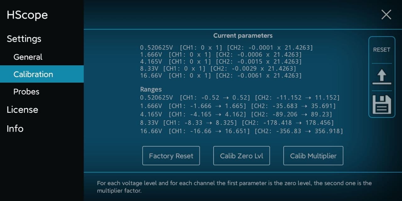
For each channel do the Calib Zero Lvl procedure in the Settings -> Calibration.
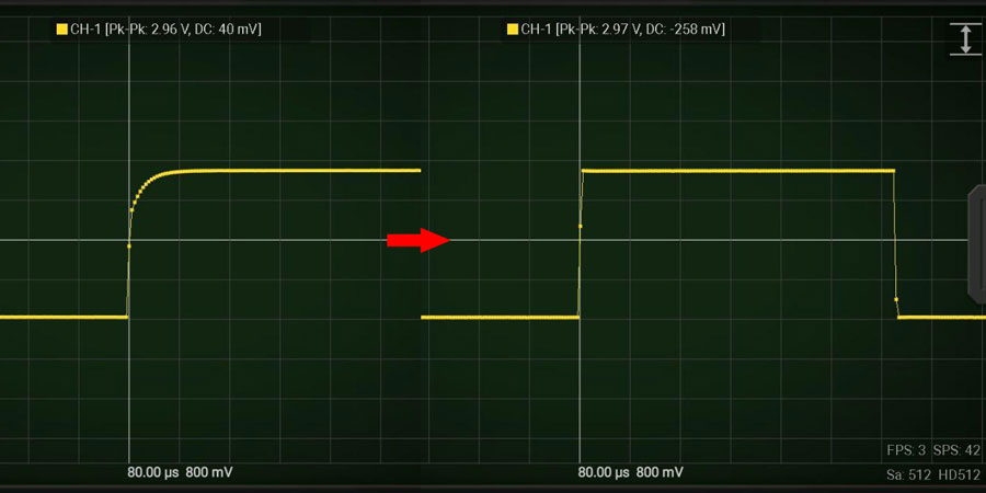
Frequency Calibration
Enable the PWM signal using the PWM module (red square icon in the right menu, then open the module). HS402 will generate a square wave on pin B15 (1kHz initially).
Connect the probe to pin B15. Use an high rate, i.e. 450KSa/s and turn the variable capacitor until the rising part of the square wave reproduce a good square. Do this for each channel.
Now the device is calibrated in frequency response.
Multiplier Calibration
For this calibration you need an accurate voltage source, for example 3.3V or 5V from a voltage stabilizer. 5V from USB port is not accurate and should never be used for this calibration. Batteries also should not be used. At least you can use LM7805 or this kind of linear voltage regulators.
For each channel do the Calib Multiplier procedure in the Settings -> Calibration.
HW Debugging
Here the tests you can perform in case of issues:
Check that PGND is approximately around 1.65V respect GND. In Option 1 the R9 trimmer requires a lot of turns to get the offset near the 0. With a multimeter you can test it reach around 1Kohm and then fine tune the zero level with HScope. A3 and A5 pins (analog inputs) also should be at the same voltage with no input signal is applied.
With a multimeter check that there are no shortcuts among the pins B3, B4, B5, B6 (these are connected to the PGA (U1, U3) which are very small and are easy to get shortcuts between the pins).
Check that voltage change on C4 and C5 when on HScope you enable/disable AC/DC option on the channels. To check that the AC/DC coupling works just apply a battery to the input. When DC is selected you should read the voltage of the battery, when AC is selected you should read 0V.
Hardware options
Hardware options in the schematics are meant to give the possibility to the user to have a lower noise by using more components. Higher option number means a better circuit.
Schematic Option 2 and 3
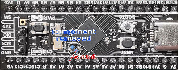
This option provide a stable reference voltage to the STM32 ADC, by installing the part indicated in the Schematic as Option 2 and 3. It requires also a modification on the STM32 board in order to bring the Vref pin from the STM32 to one of the pins of the development board (PA2). One component should be removed (the inductor) and a jumper should be created to PA2 according the picture under. PA2 is inactive and used just to provide the Vref signal. Demo video here.
Option 2 just show a greater cross-channel noise respect Option 1: 0.25% vs 0.05%.
Note: after this modification the STM32 board will work only if 3.3V is applied to PA2 (now Vref)!
Arbitrary Input Range
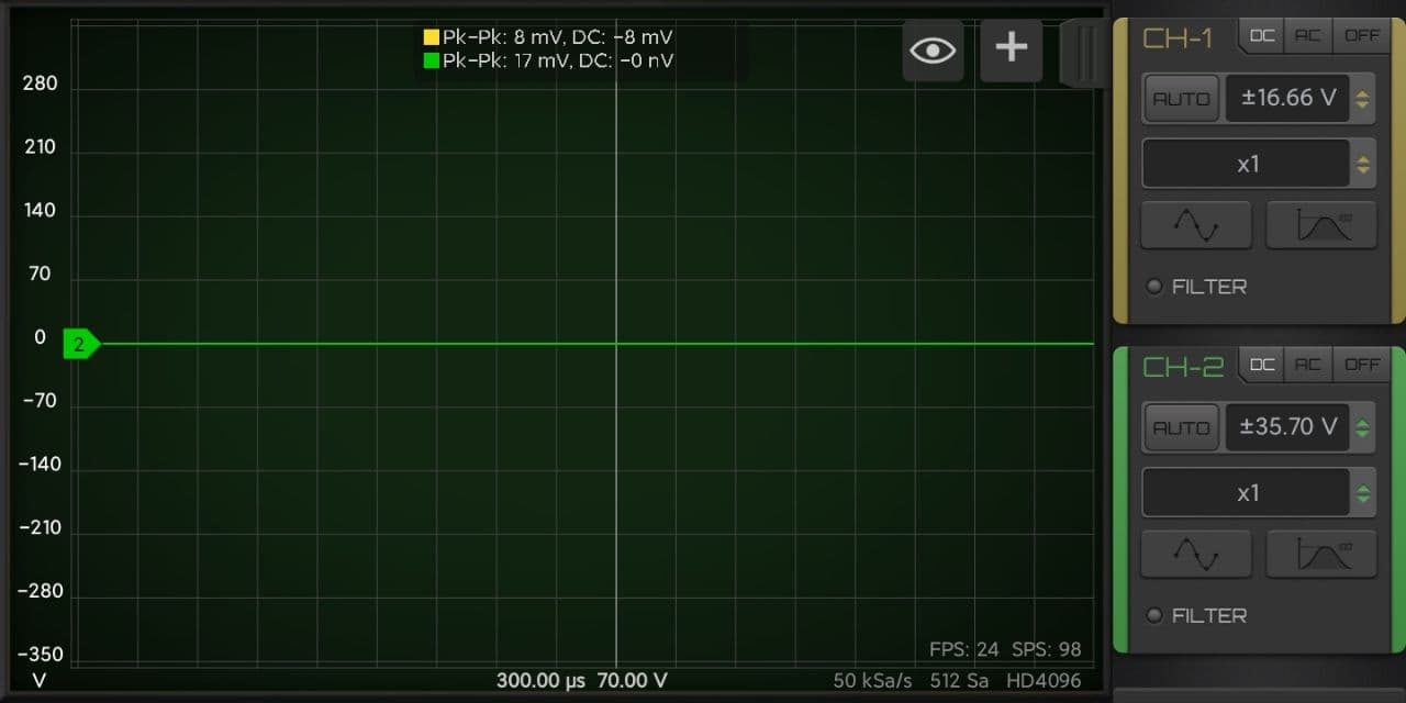
You can design the input ranges for each channel according your needs. For example it is possible to have the maximum voltage to ±5V or to ±50V. Channel input ranges can be also different (for example a channel has max voltage ±16V and the other channel ±5V).
Calculate R2/R3 (or R6/R7) resistors values according the required range. Pay attention the sum of these 2 resistor should be around 1Mohm. a) R2 + R3 = 1Mohm b) ±Range = 1.65 * (R2 + R3) / R3 Example: Range = 1.65 * (910k + 100k) / 100k = ±16.66V
Do the multiplier calibration of the channel. After the software will show the voltage ranges according the hardware.
Warning: do not exceed 50V input range since the input is not isulated from GND and from the phone, leading to a possible electrocution.
The following tests are referred to PCB V3.0 without any box. Hardware option 3 (lowest noise).
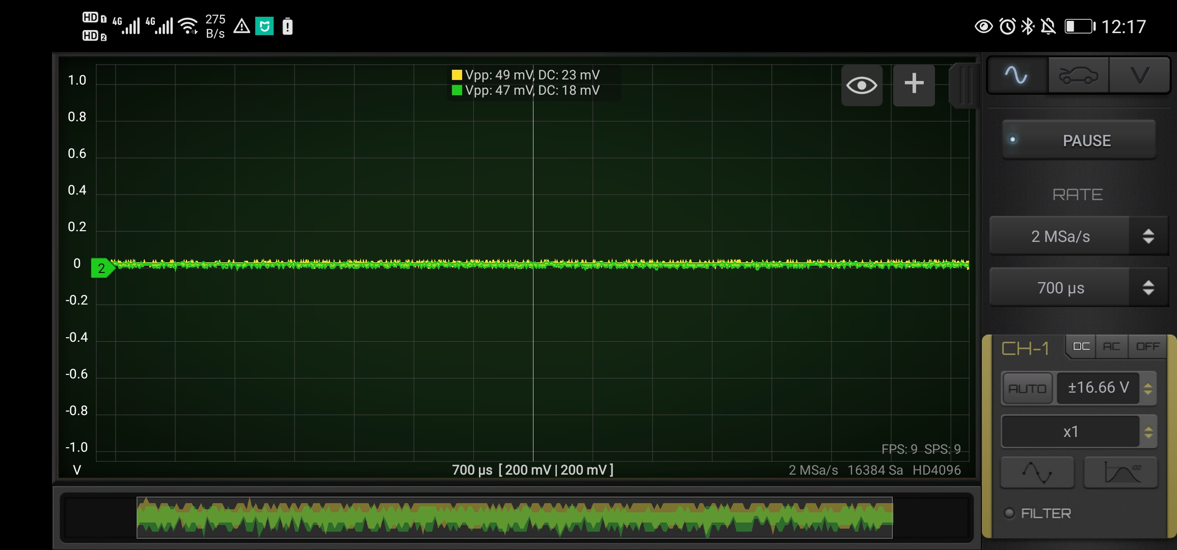
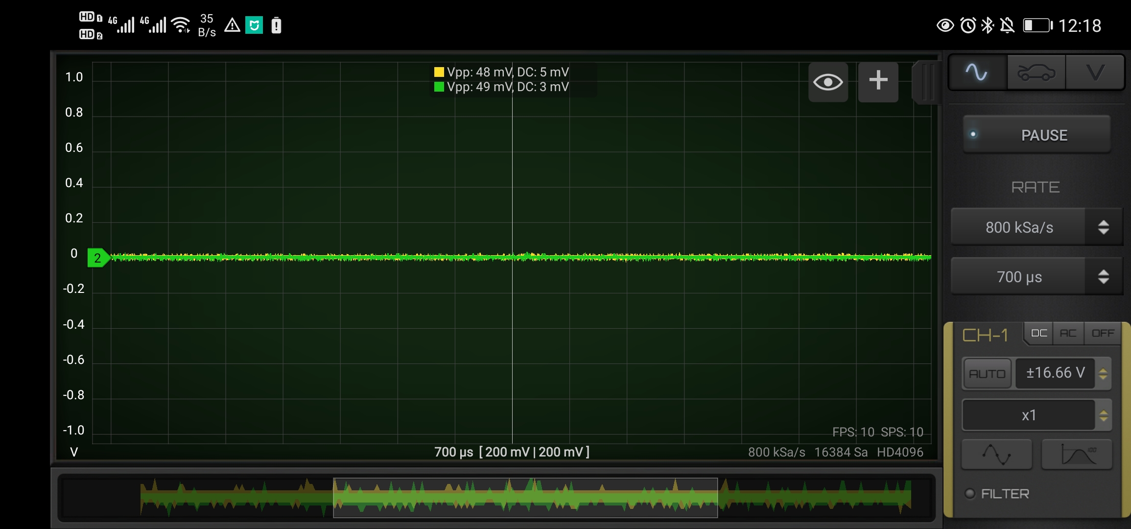
Base Noise Analysis
Tests performed without probe, open BNC connectors.
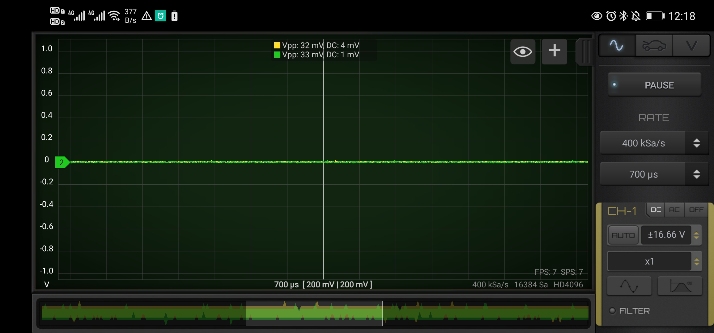
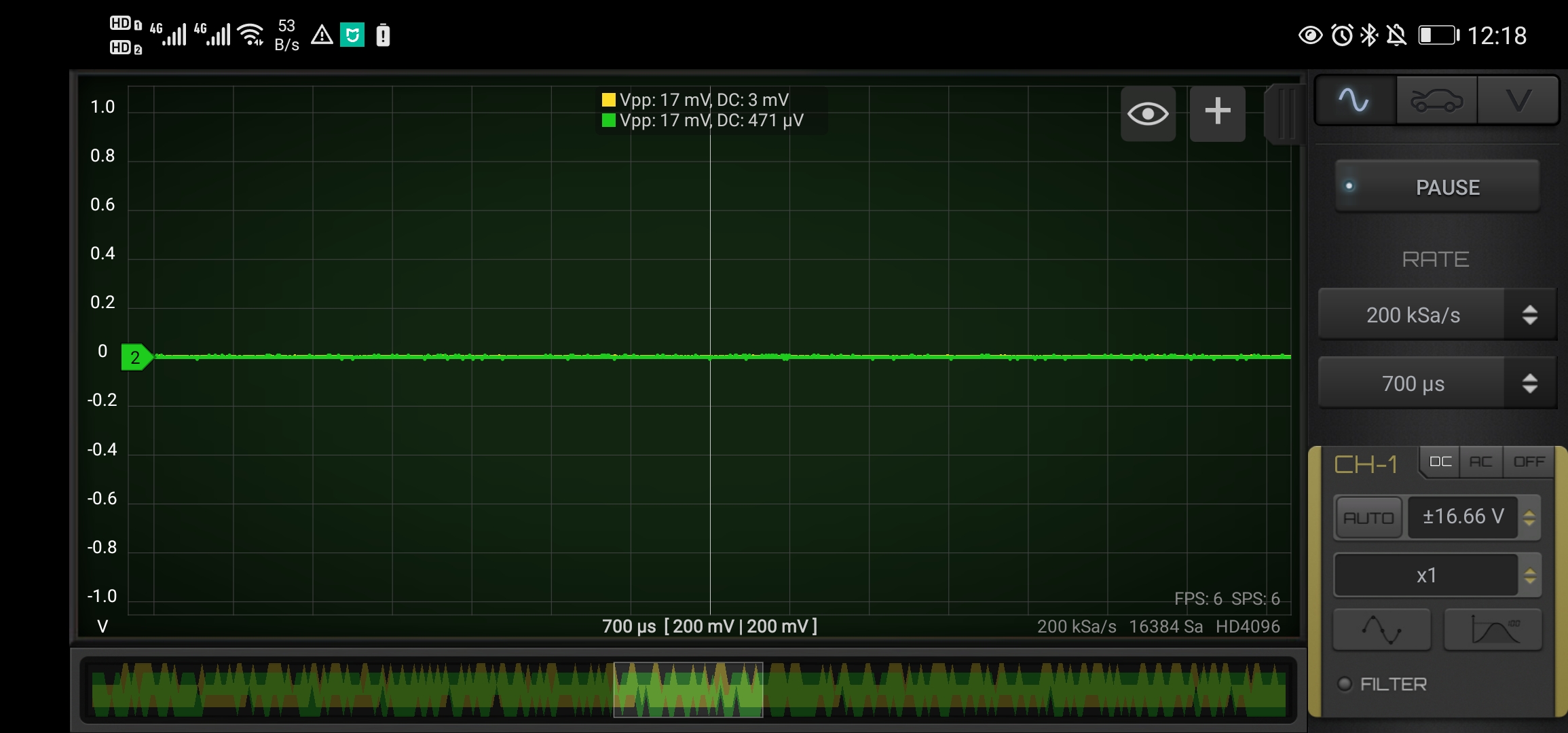
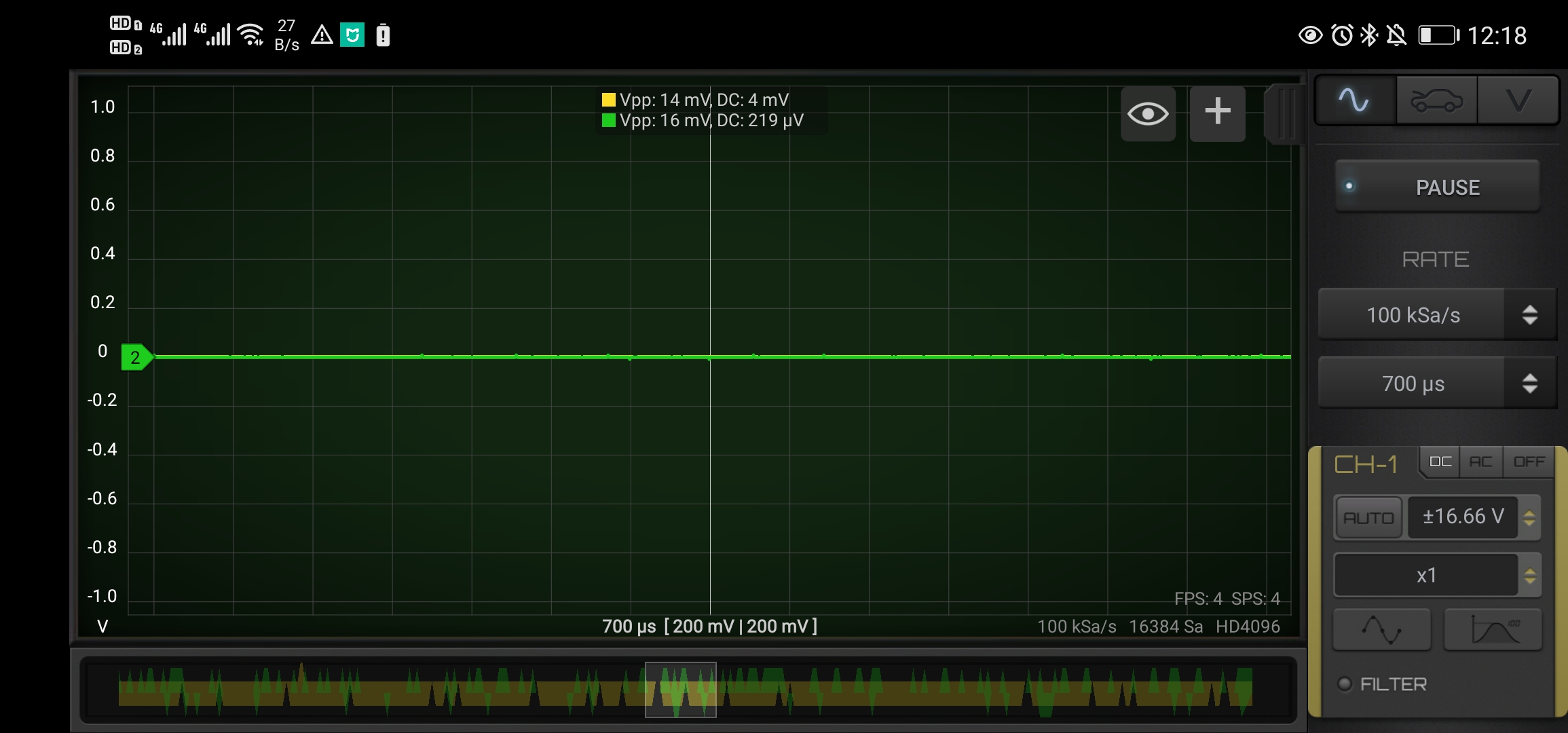
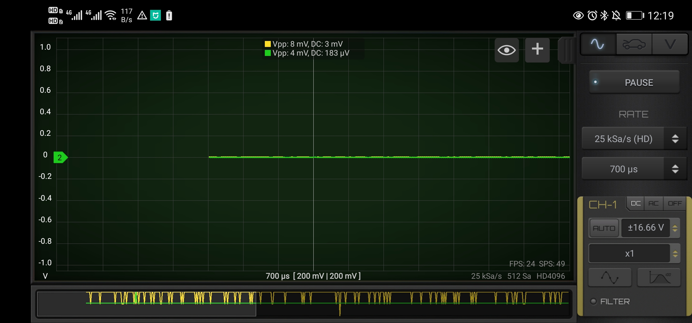
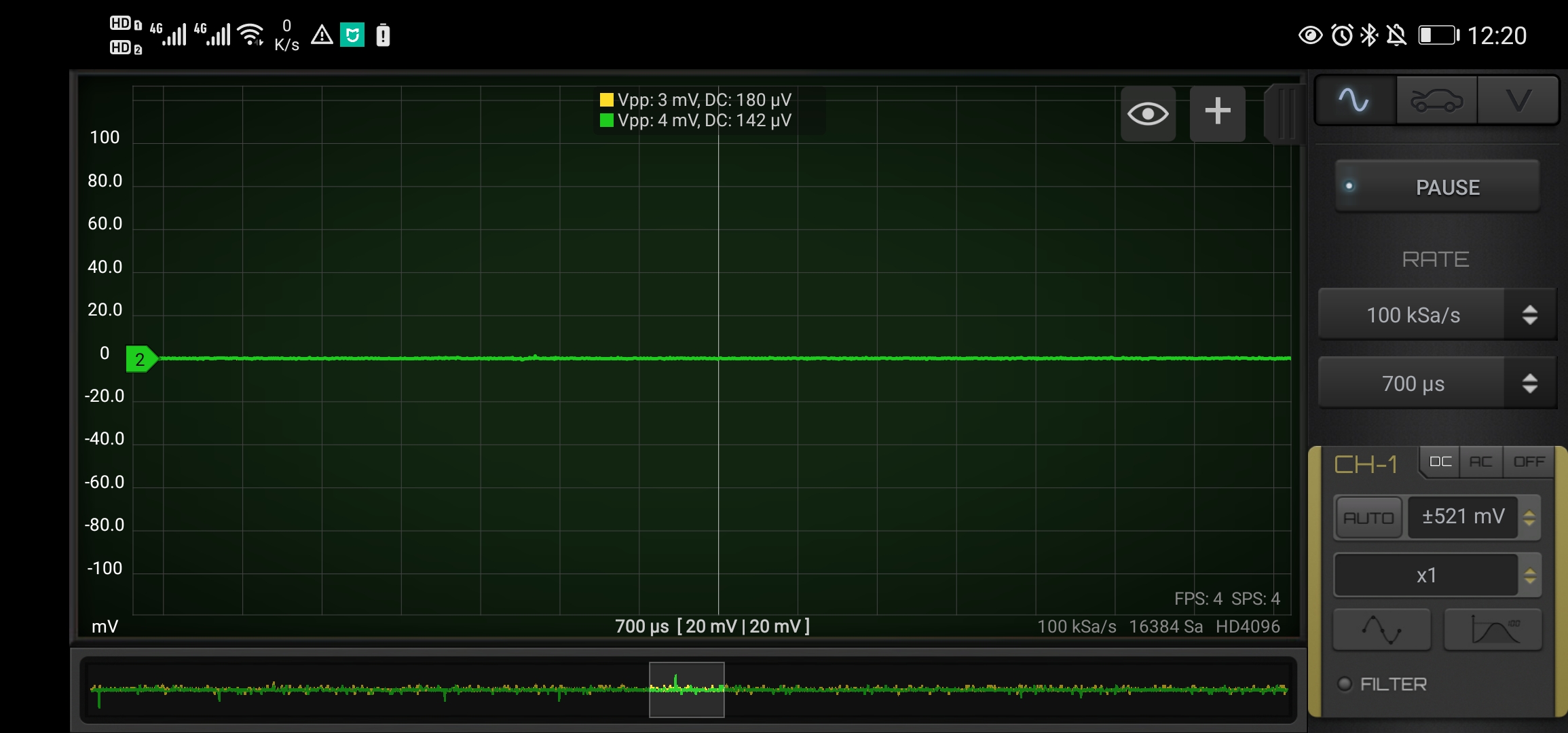
Noise at highest voltage range
This test shows the following base noise:
@2MSa/s 0.15%
@400kSa/s 0.1%
@200kSa/s 0.05%
@50kSa/s 0.02%
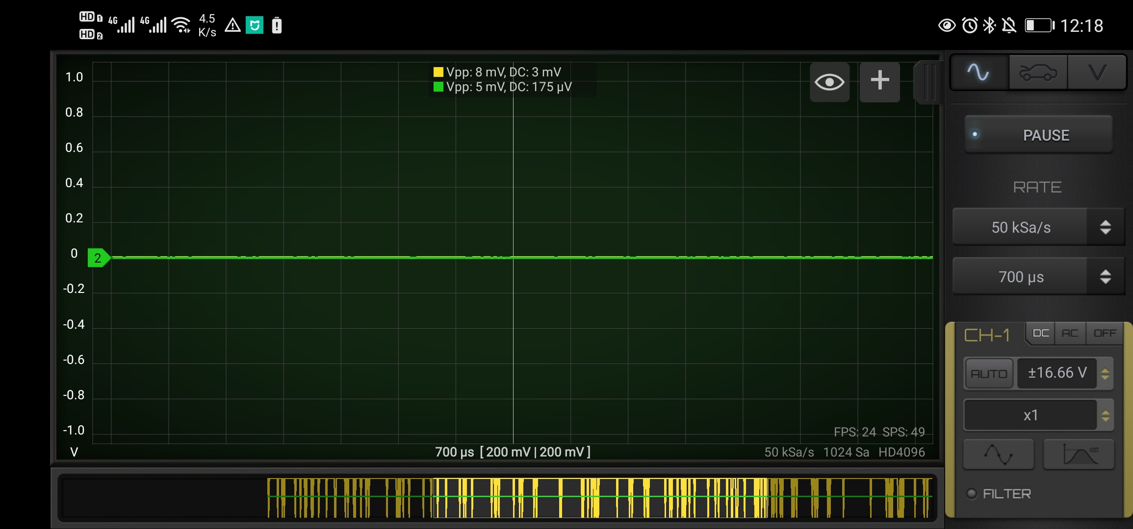
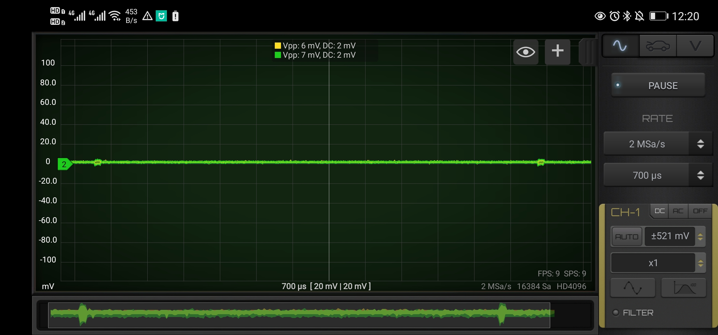
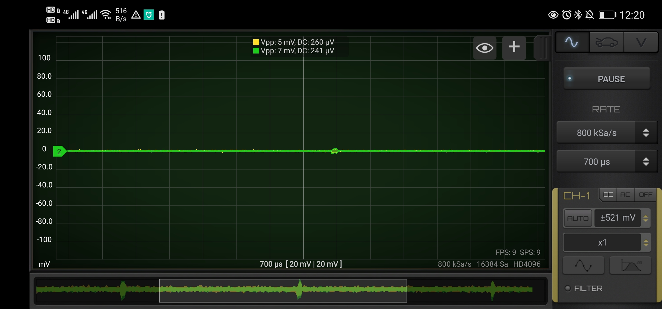
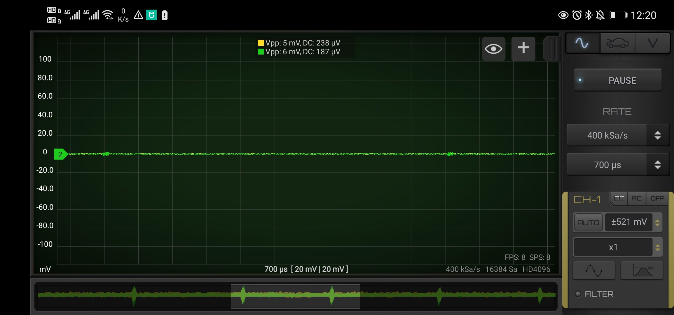
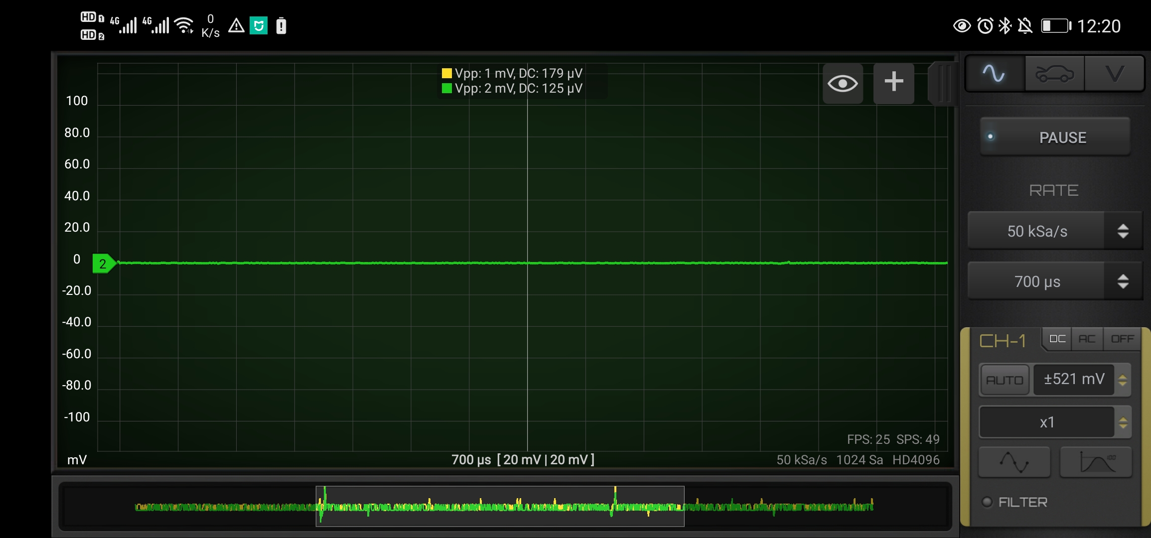
Noise at lowest voltage range
This test shows the following base noise:
@2MSa/s 0.7%
@100kSa/s 0.4%
@50kSa/s 0.2%
@25kSa/s 0.08%
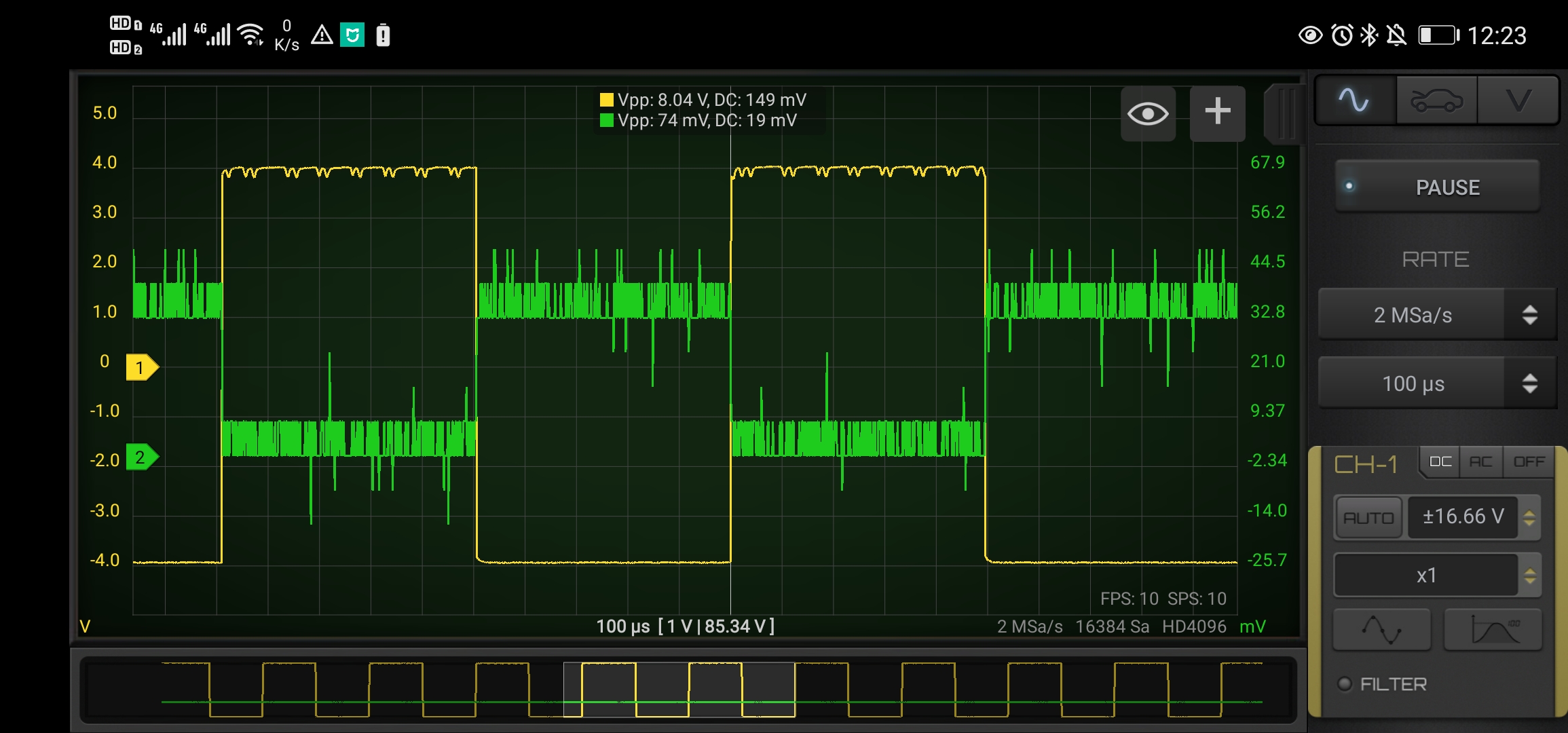
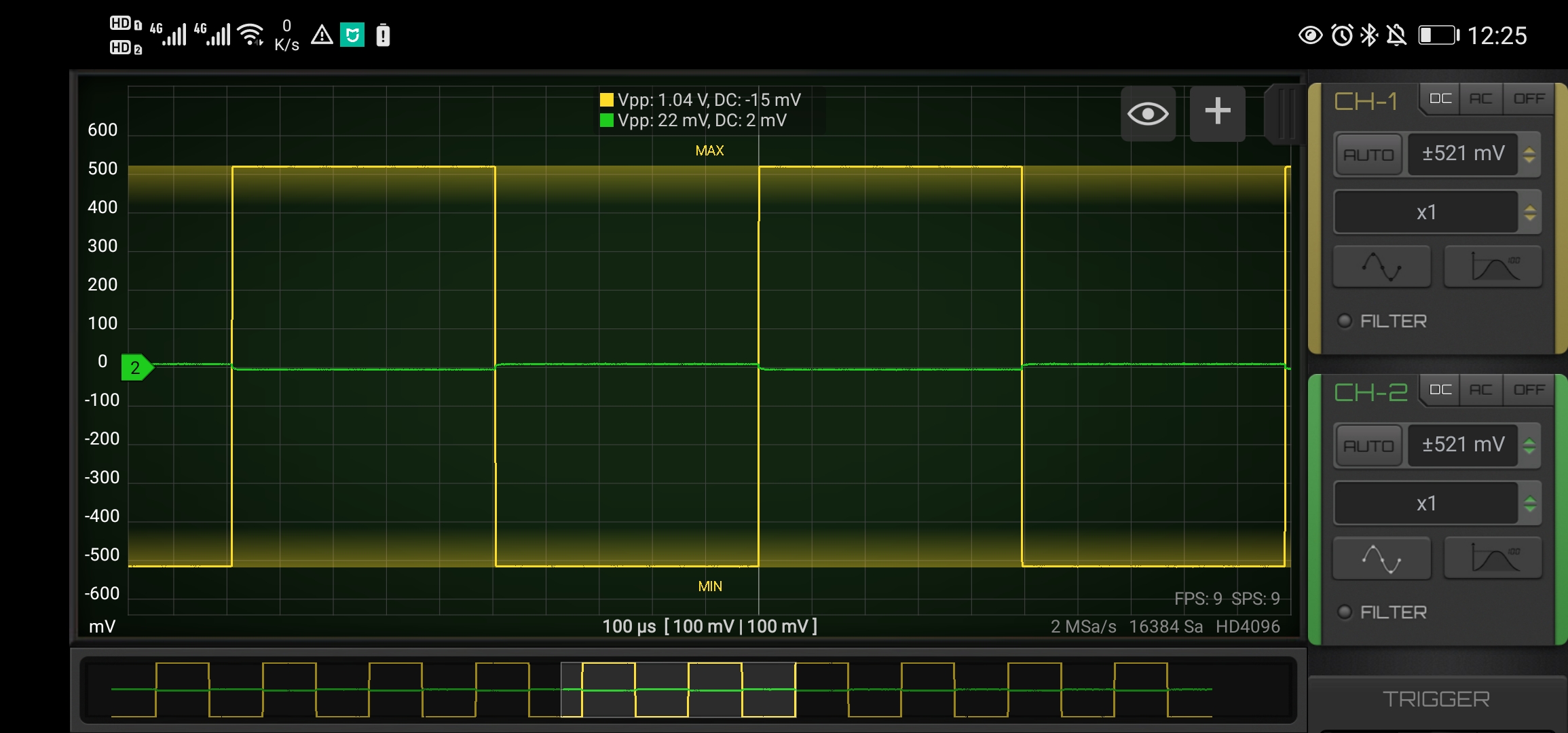
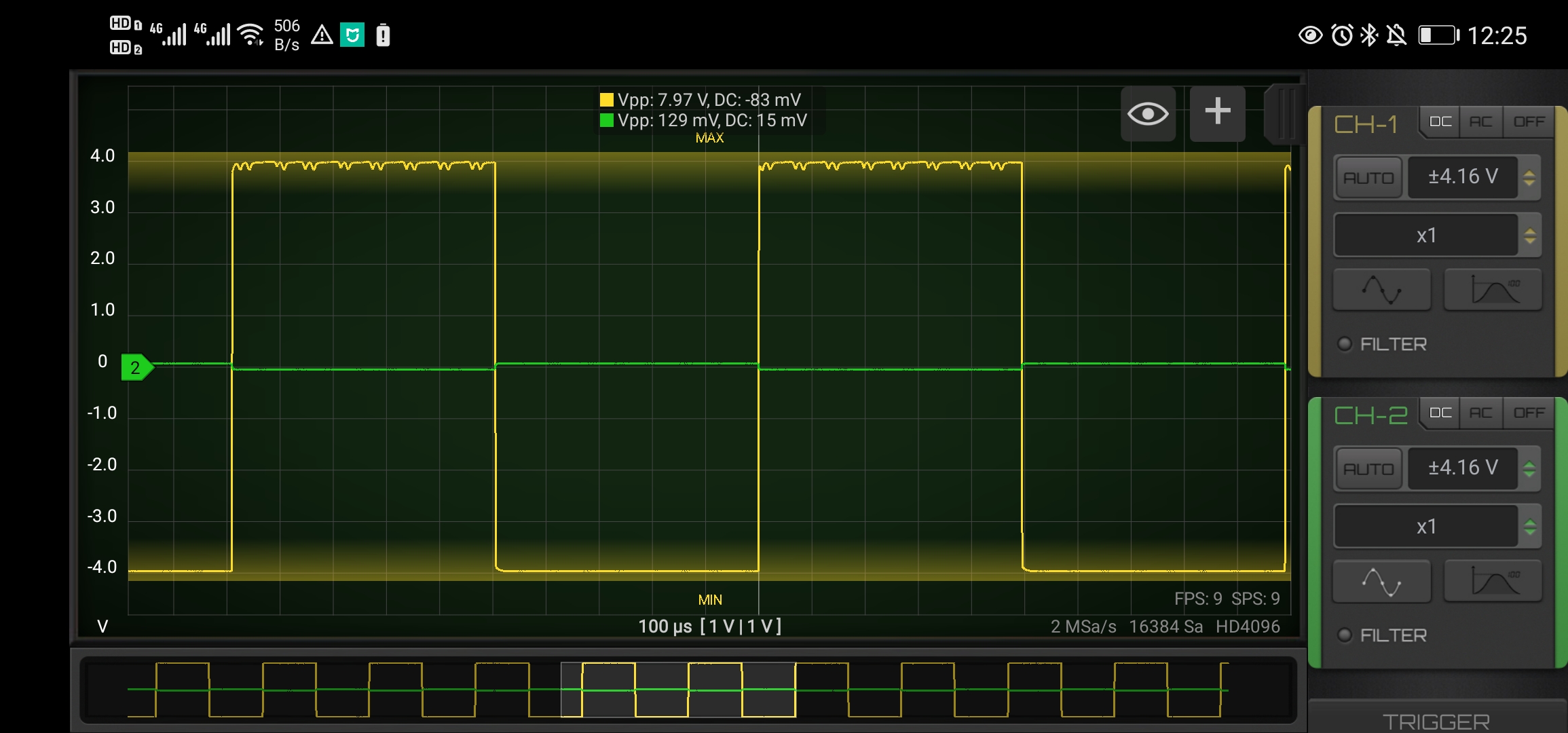
Cross channel noise
Cross channel noise is present. Part of the signal of one channel can be found on the other channel as noise.
When one of the channel saturates (input voltage greater than the maximum range) then the cross channel noise is greater. Channel saturation should be avoided during use.
In the following examples cross channel noise can generate a noise up to 0.5%. At the same conditions without cross noise the base noise would be 0.15%.
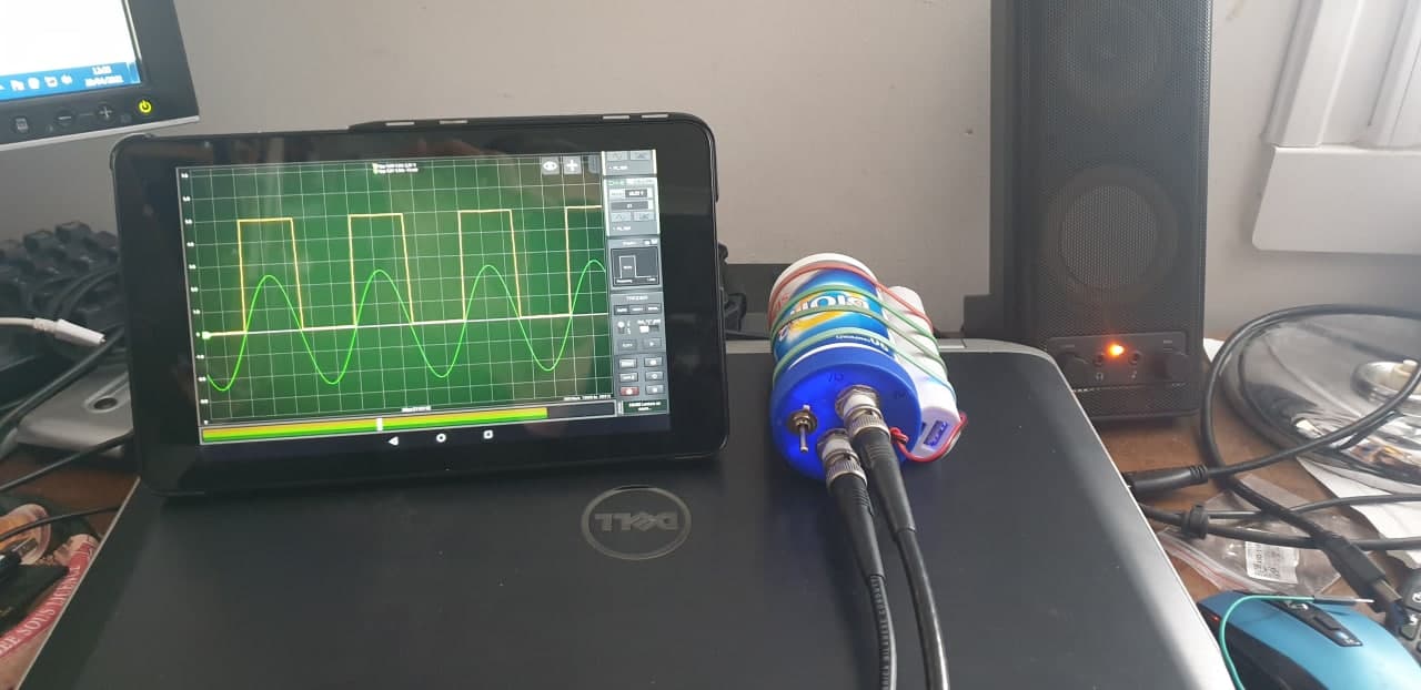
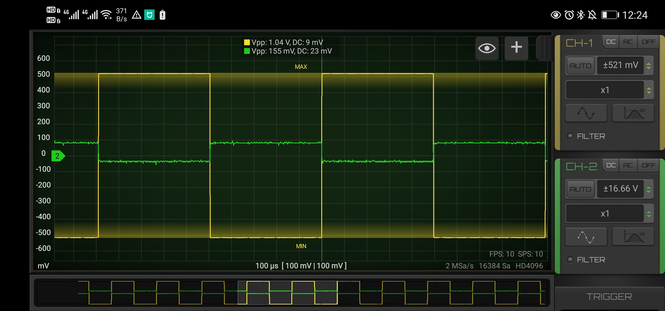
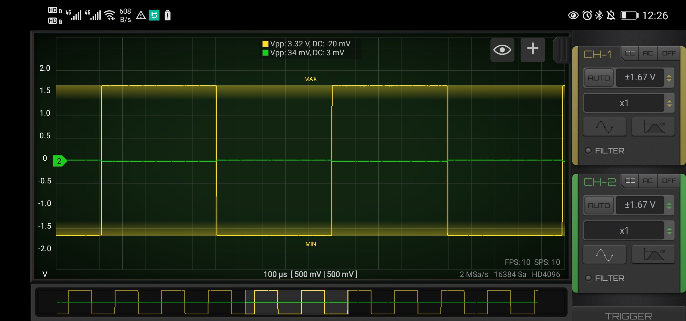
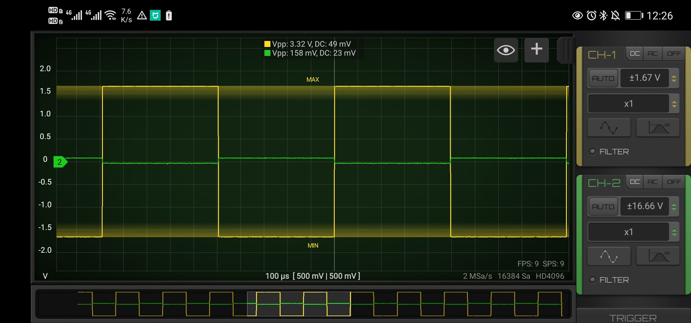
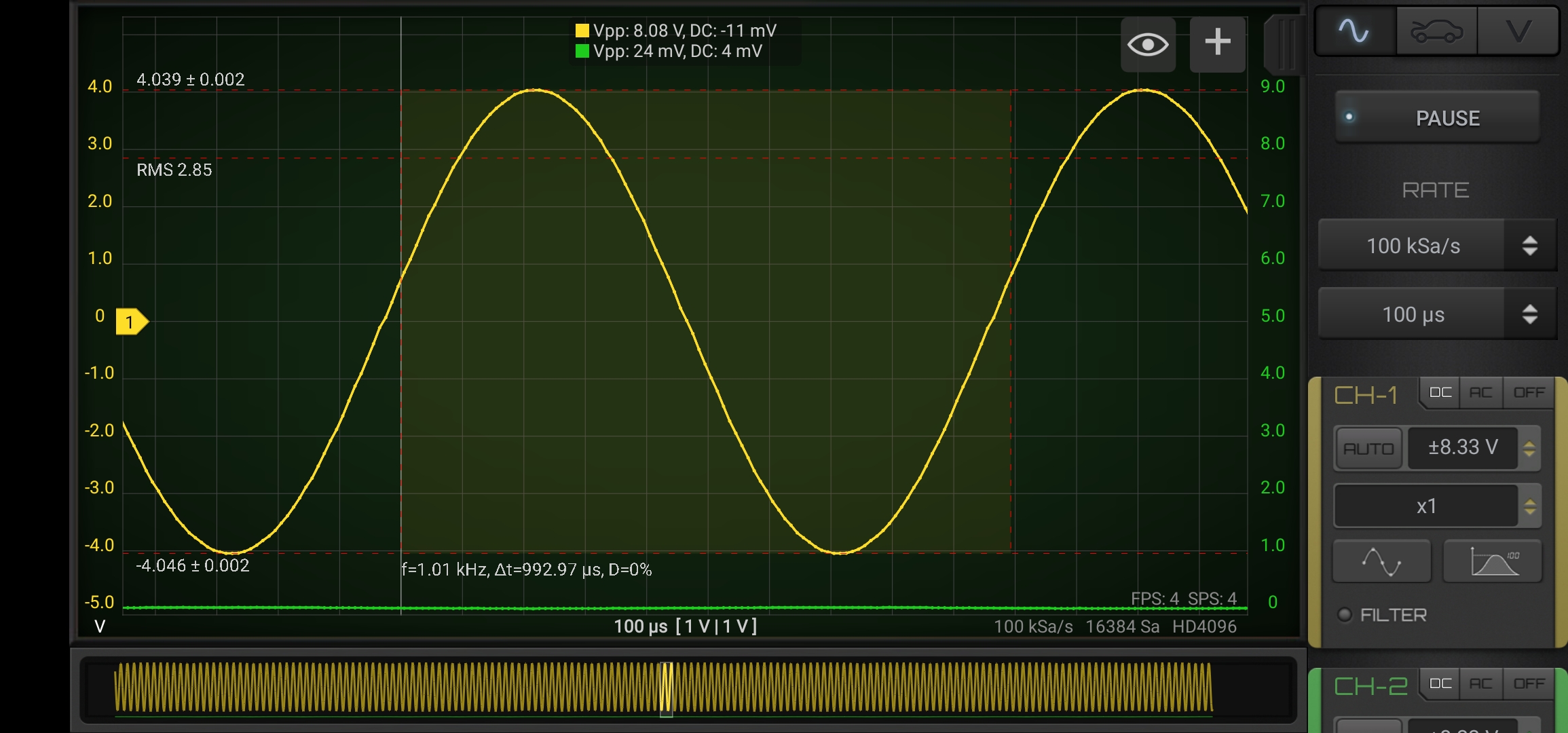
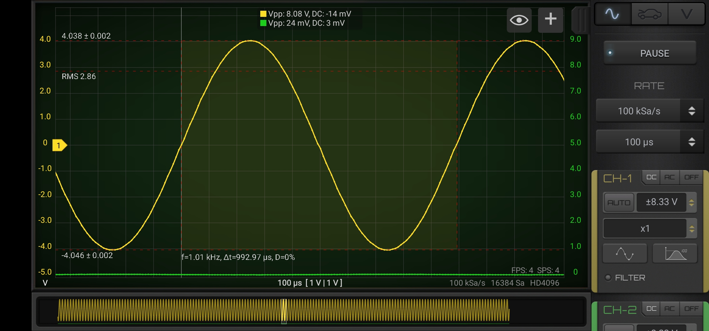
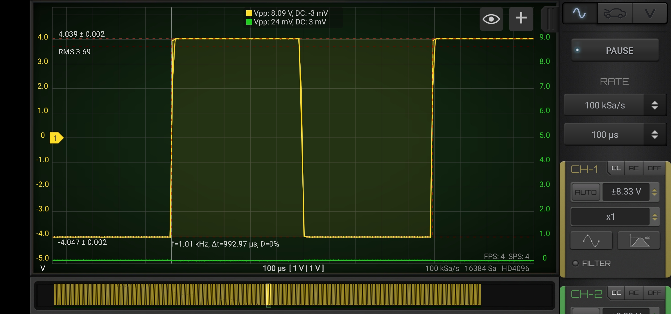
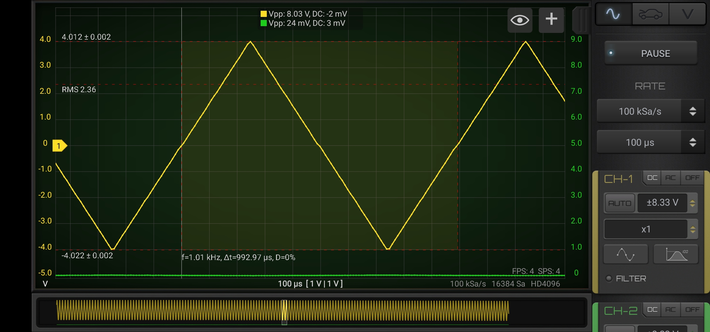
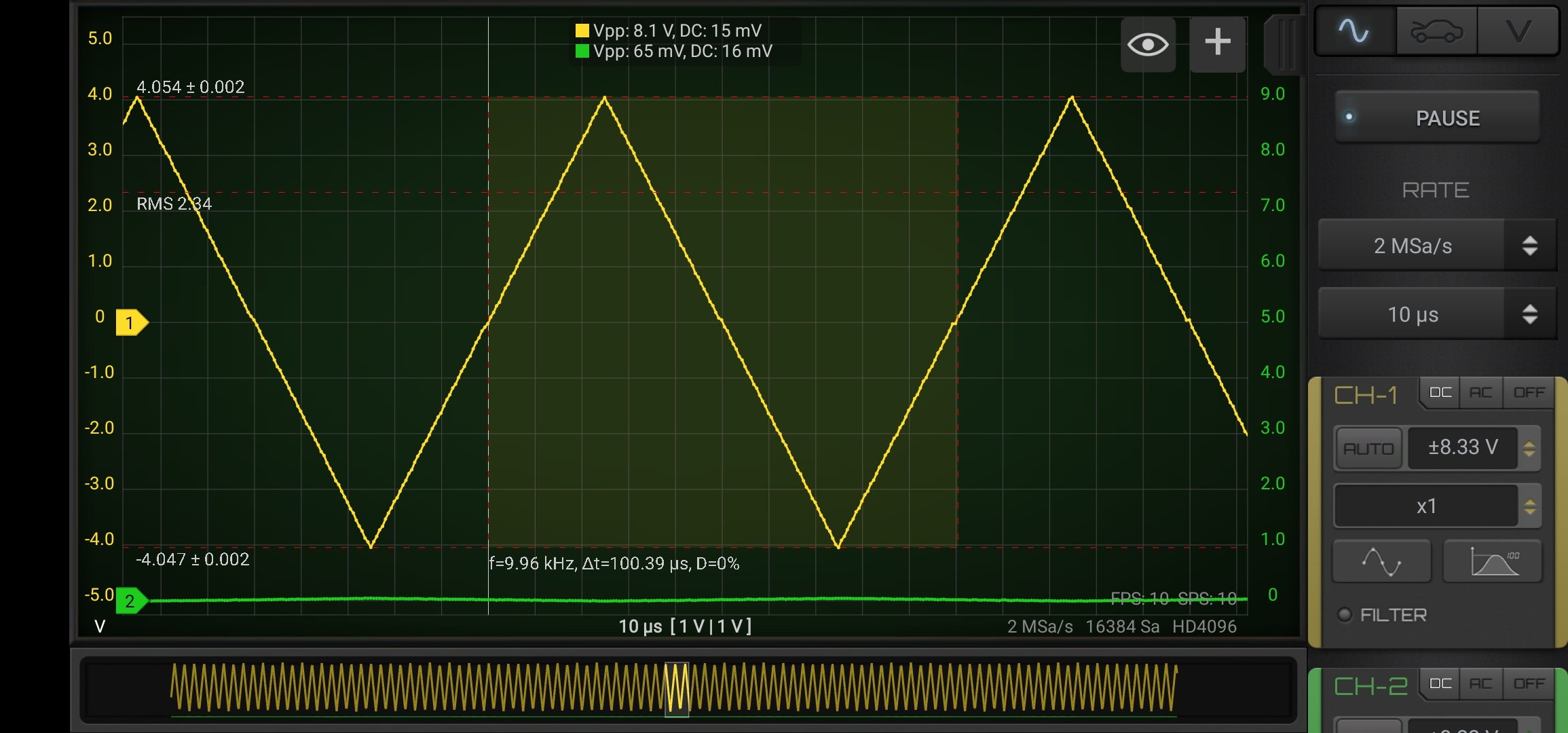
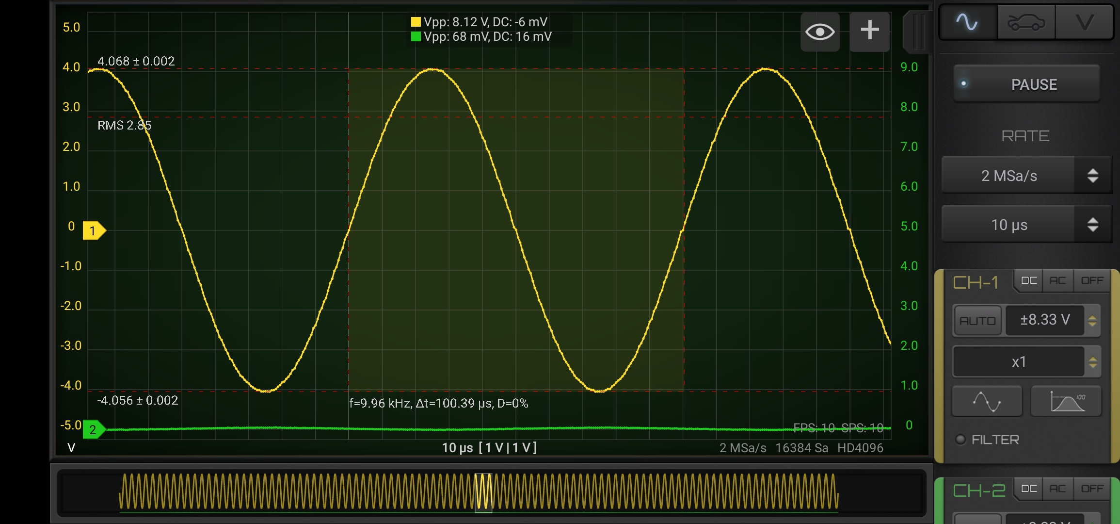
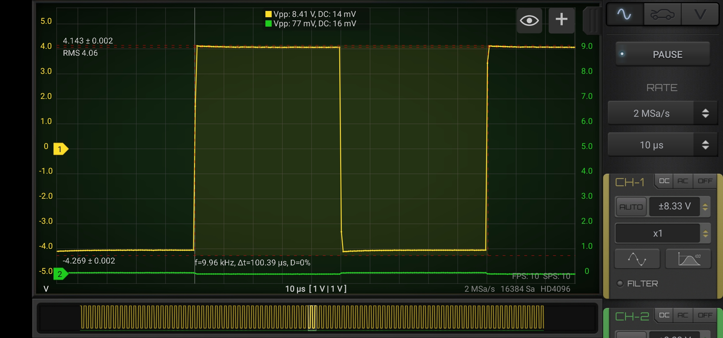
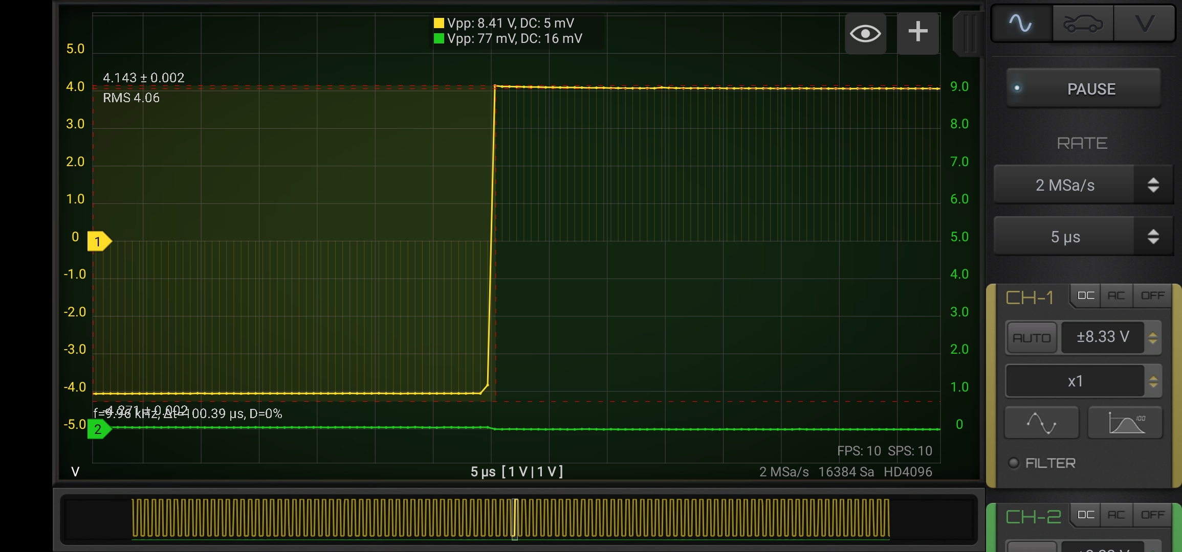
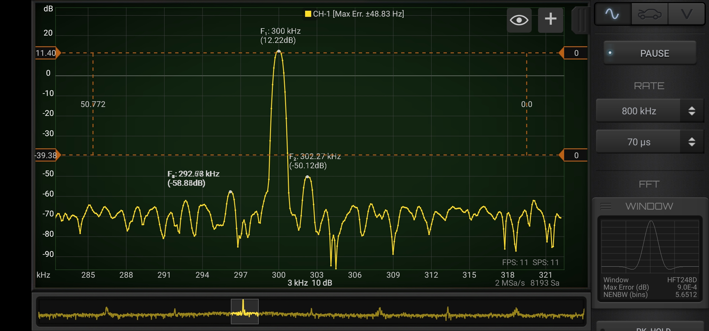
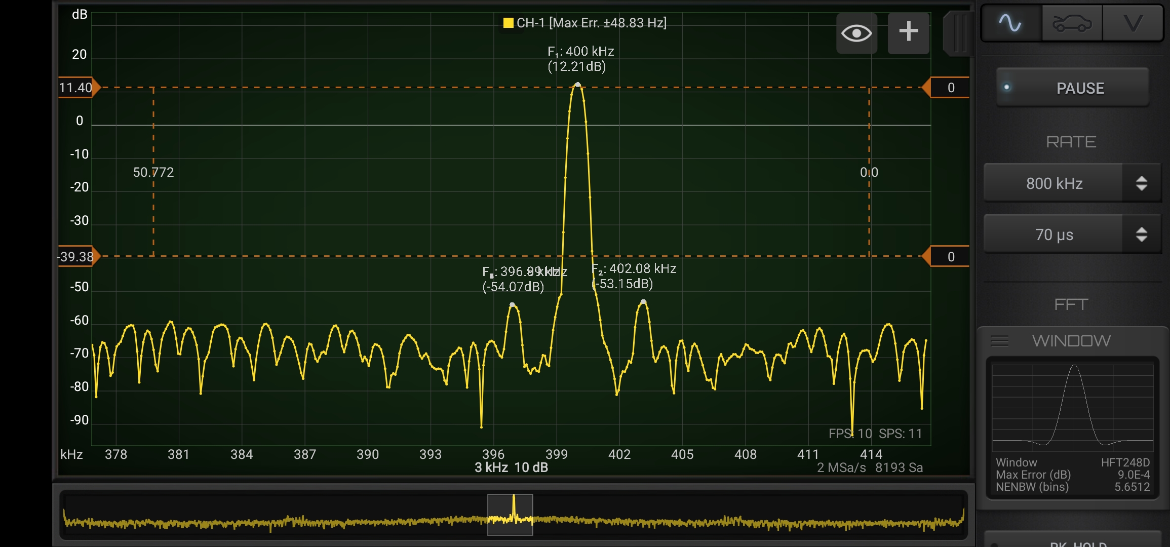
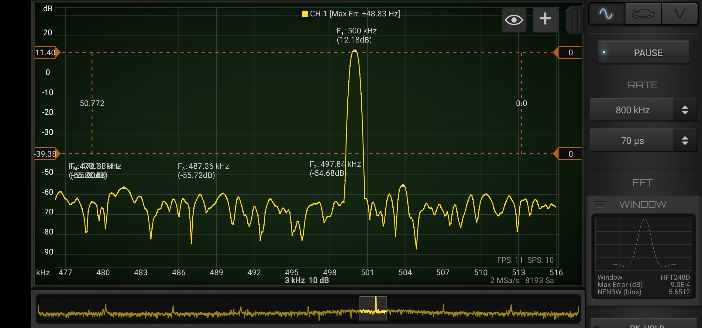
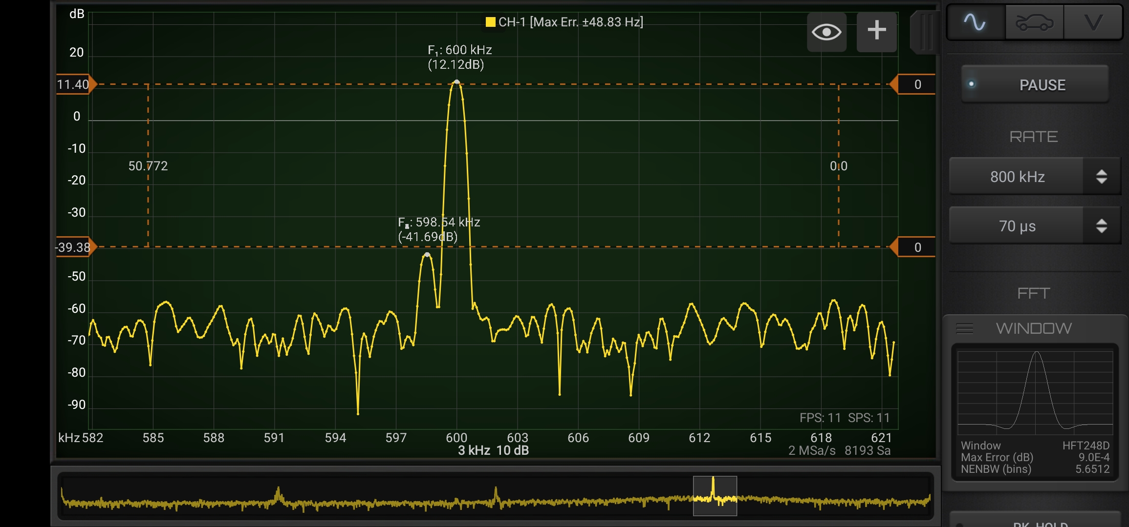
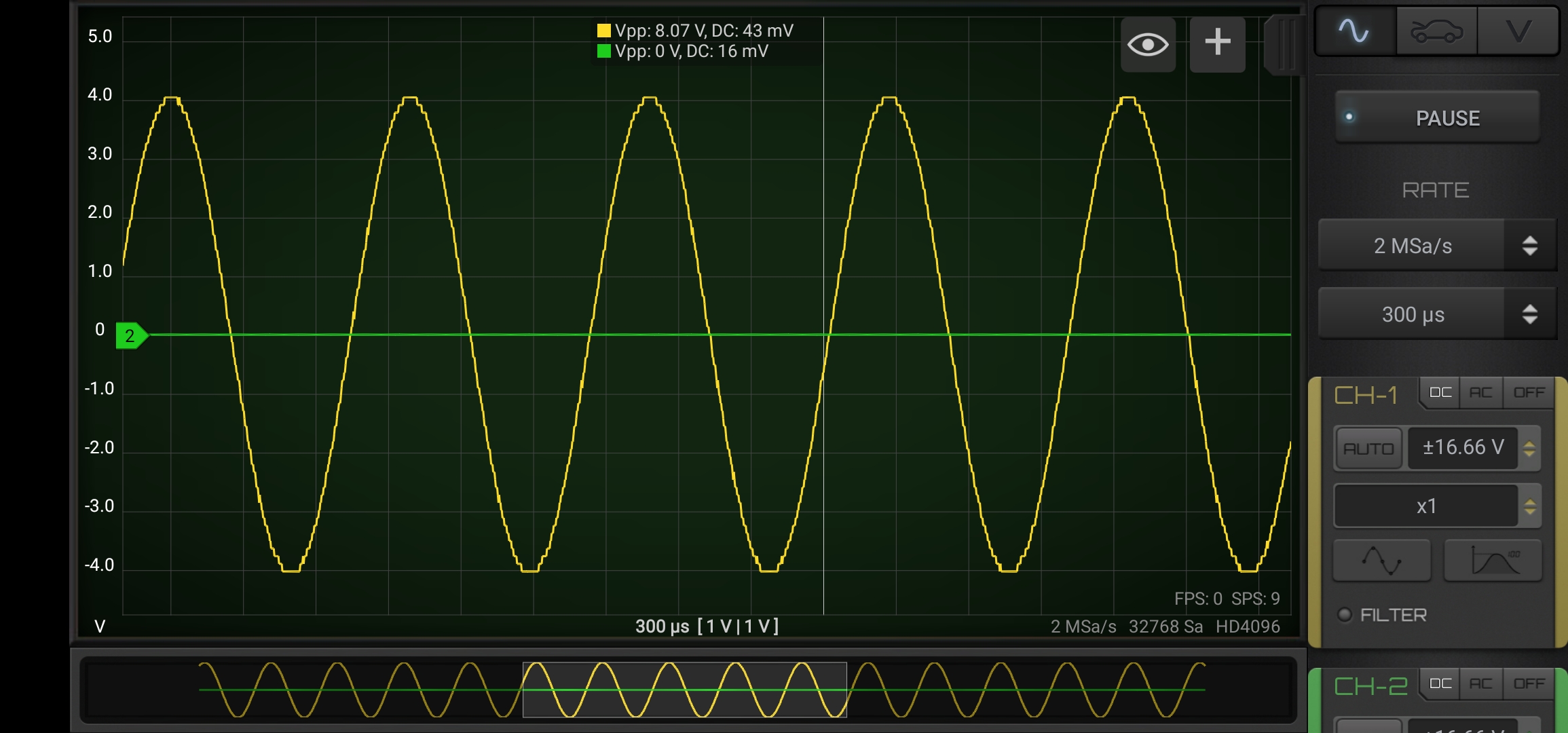
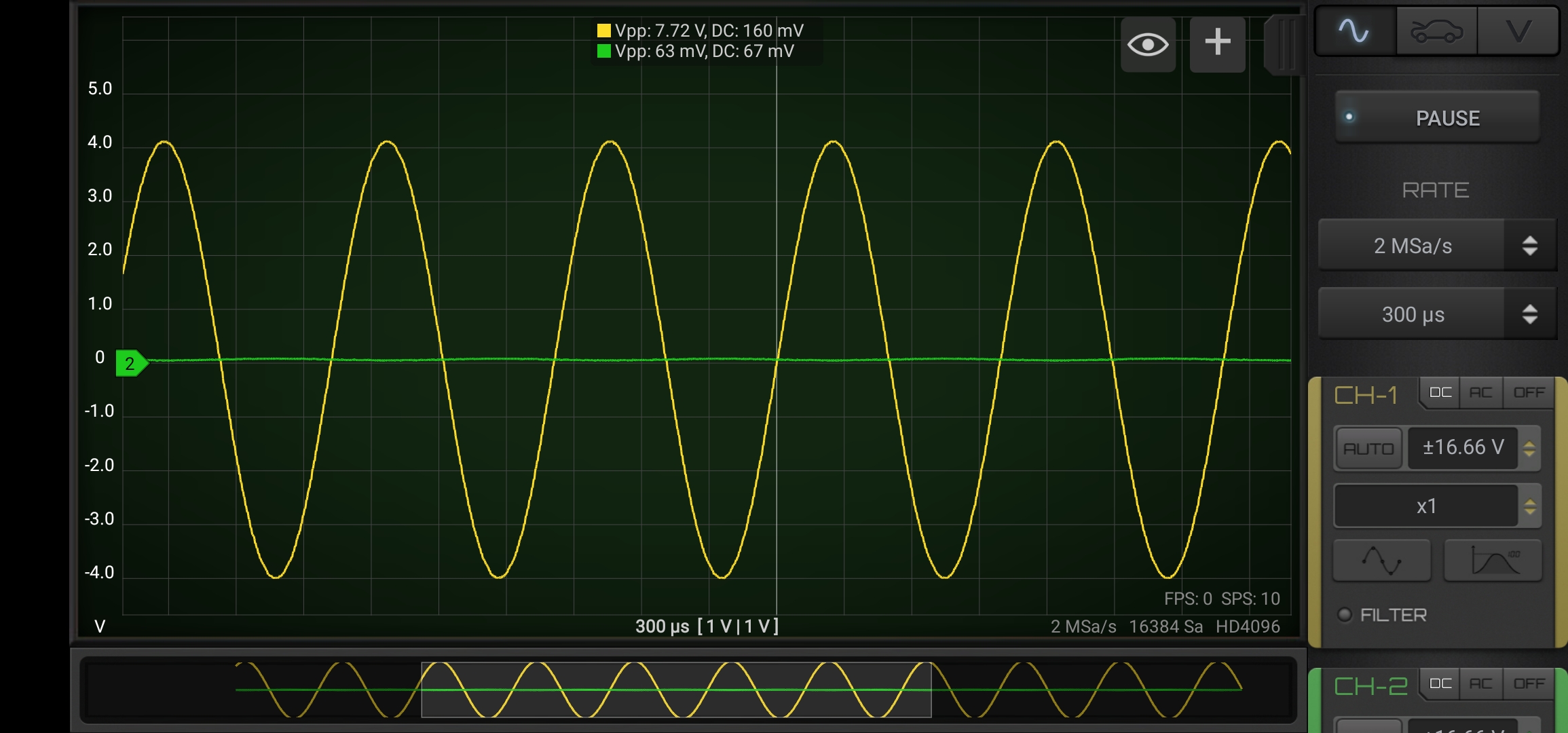
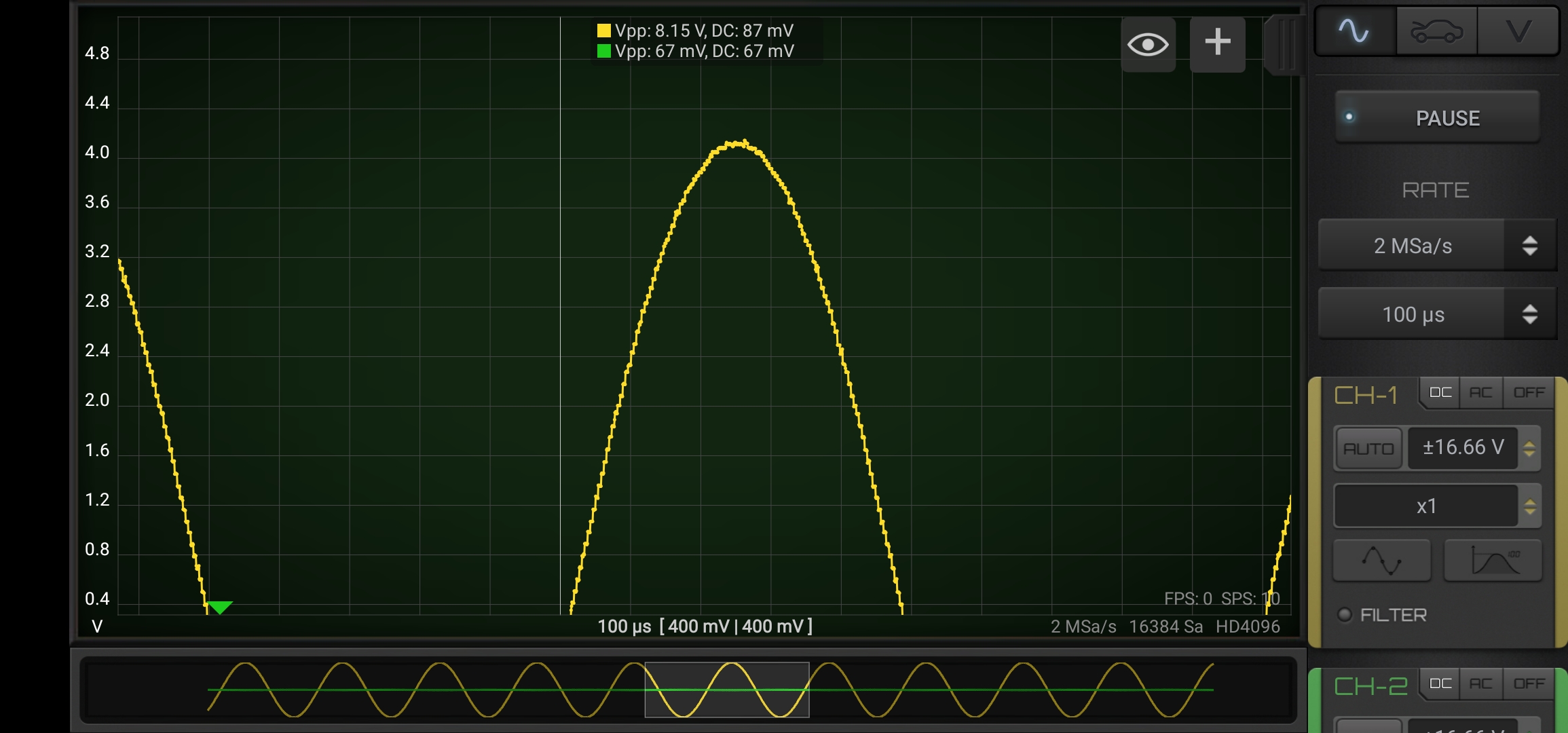
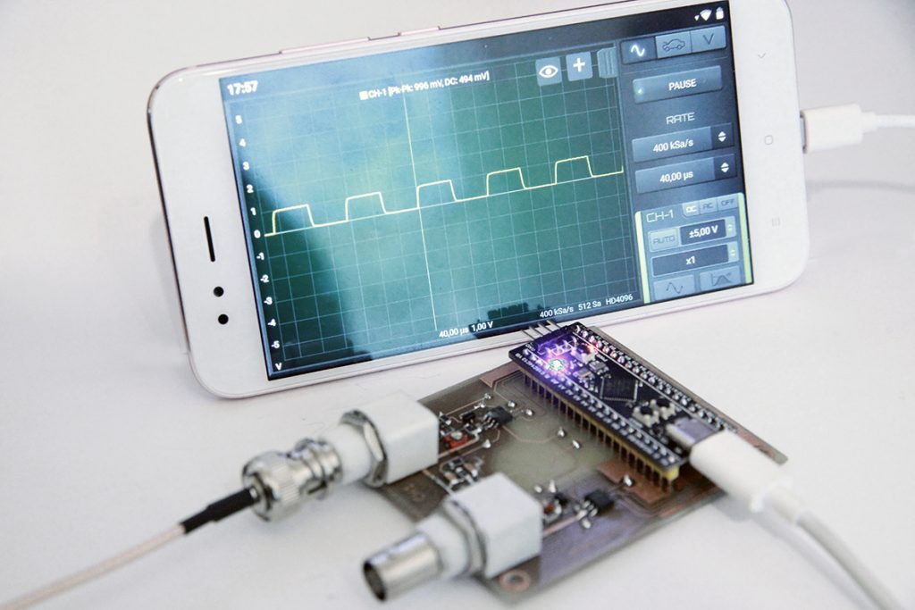
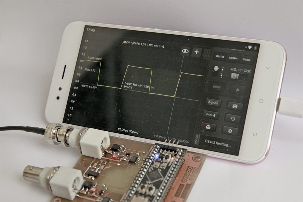
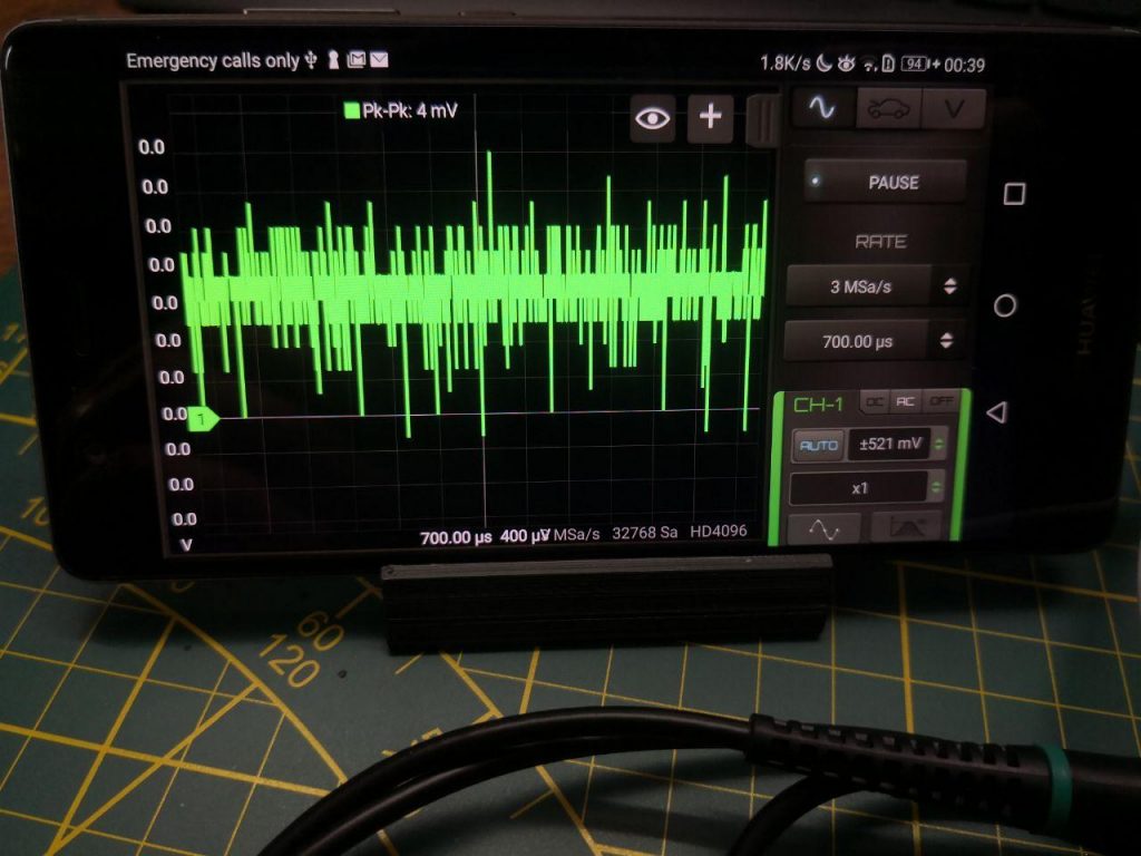
Sample Waveforms
Sample signal acquisition from a signal generator after calibration.
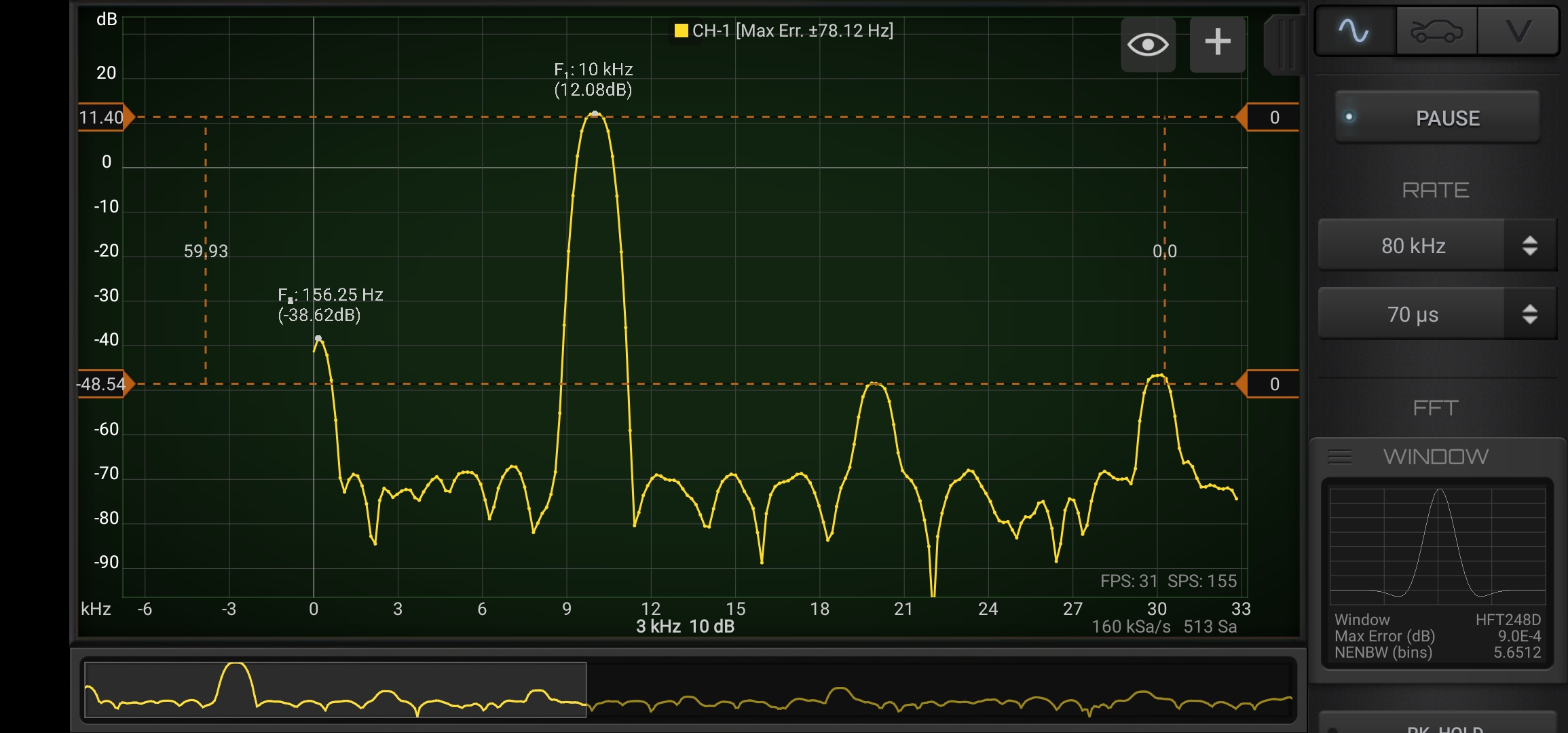
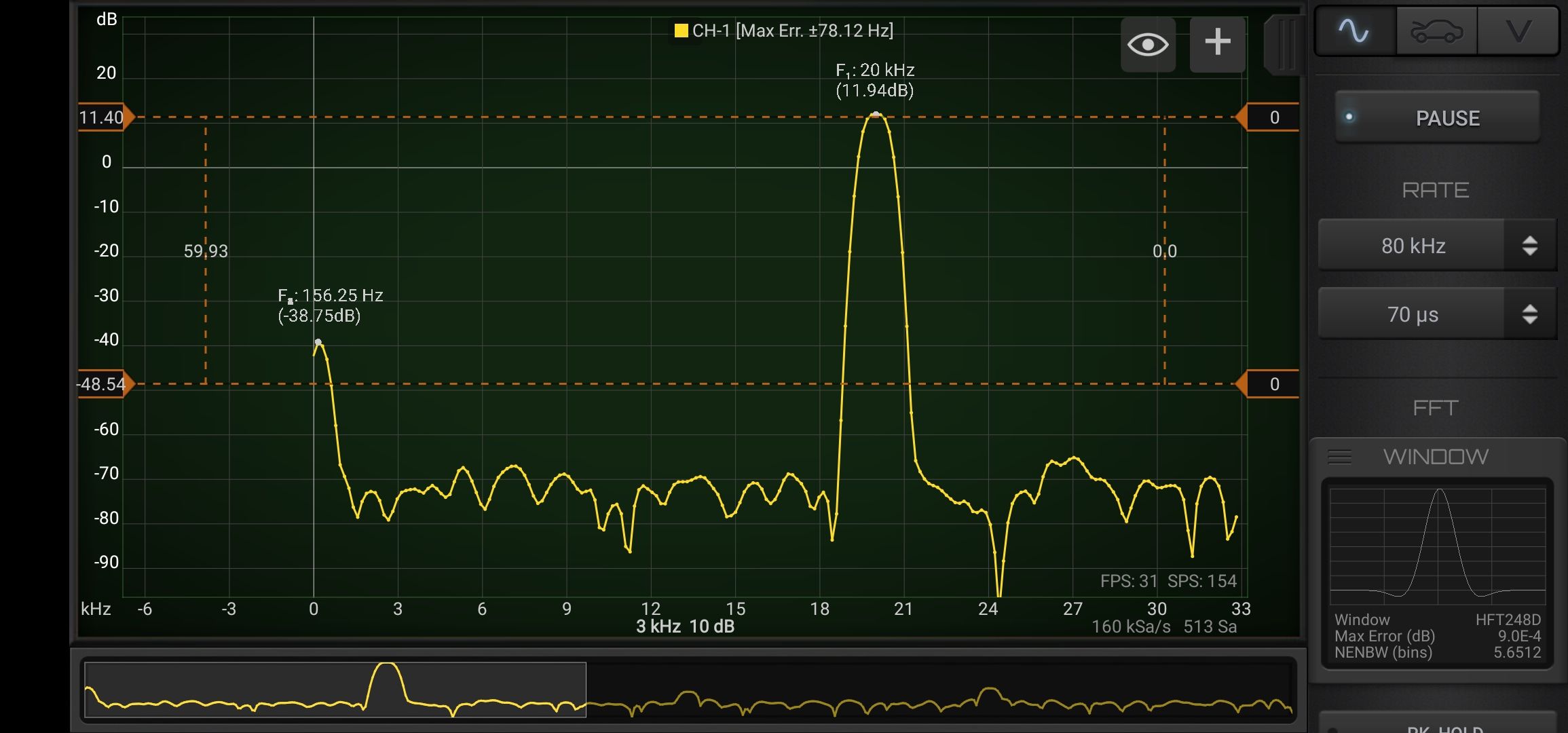
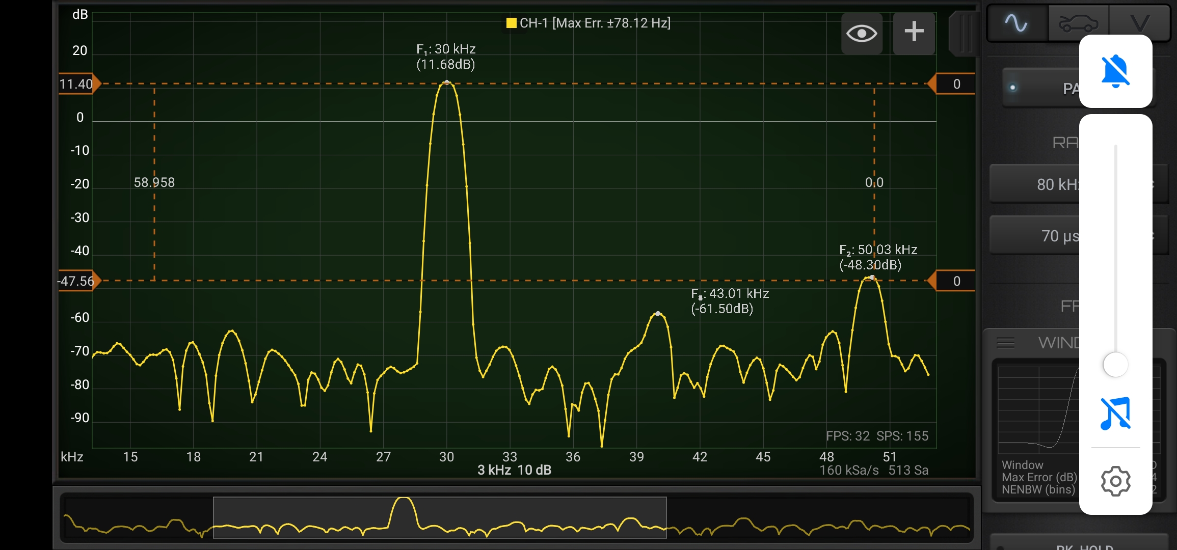
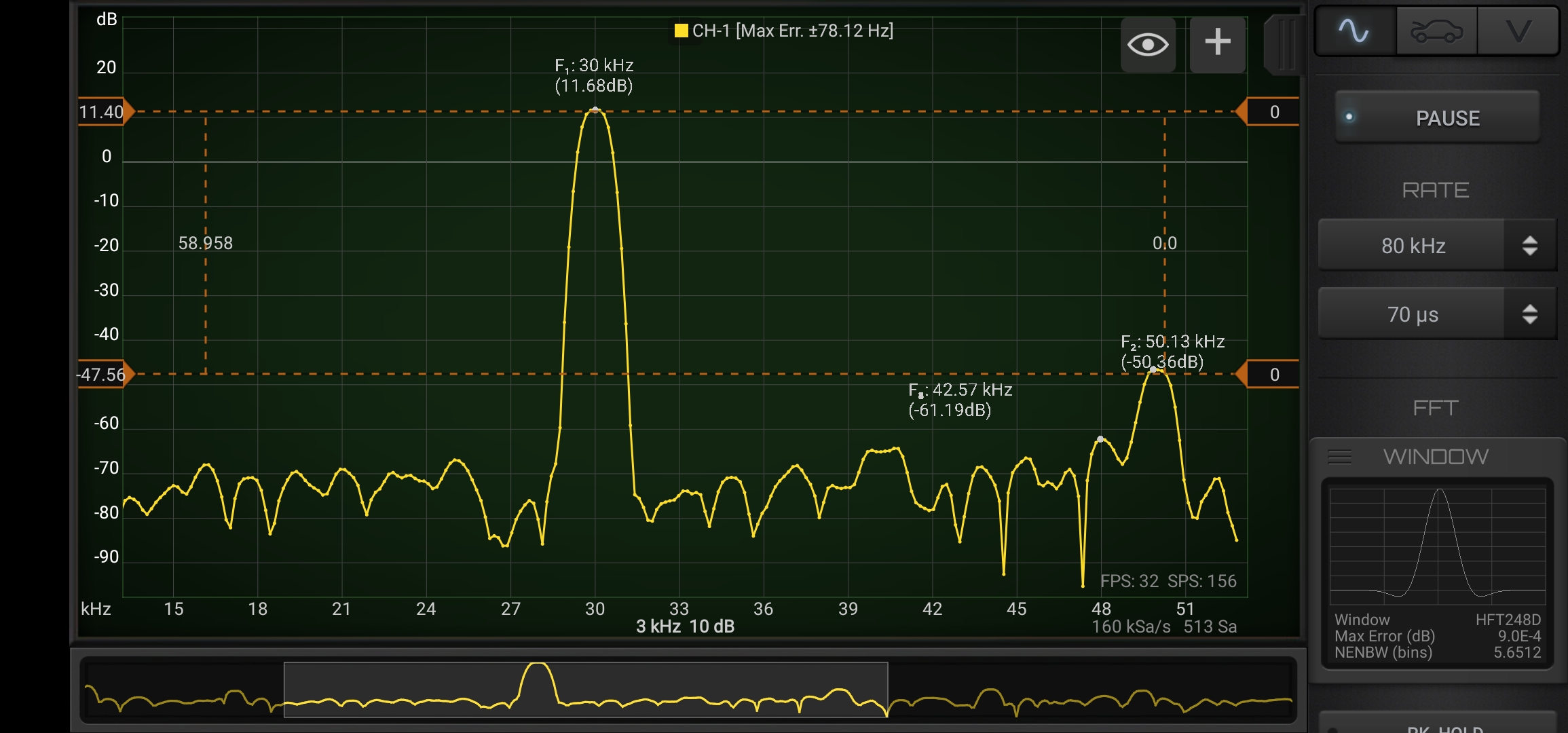
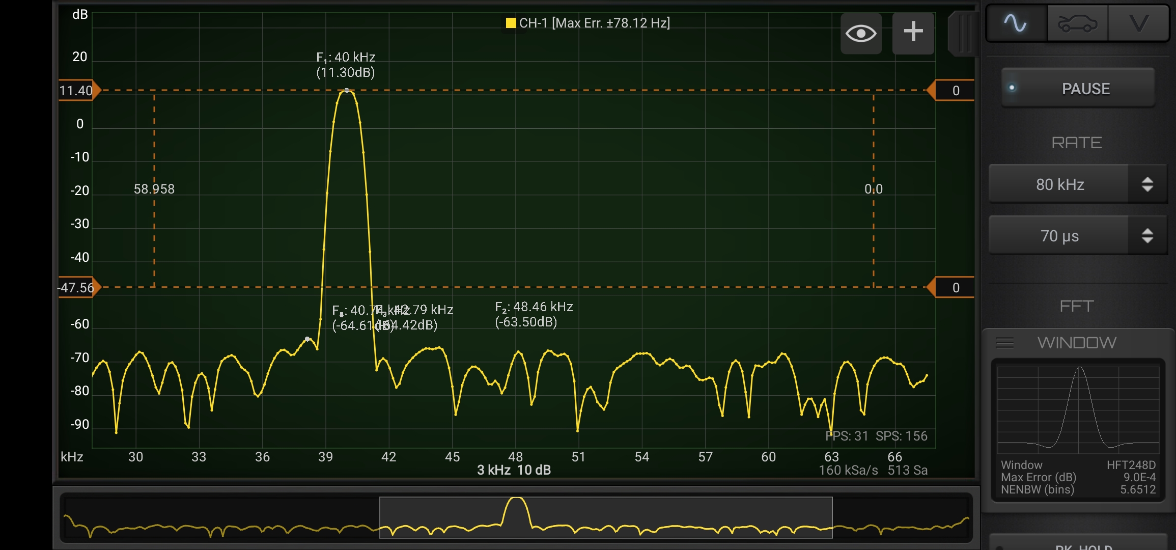
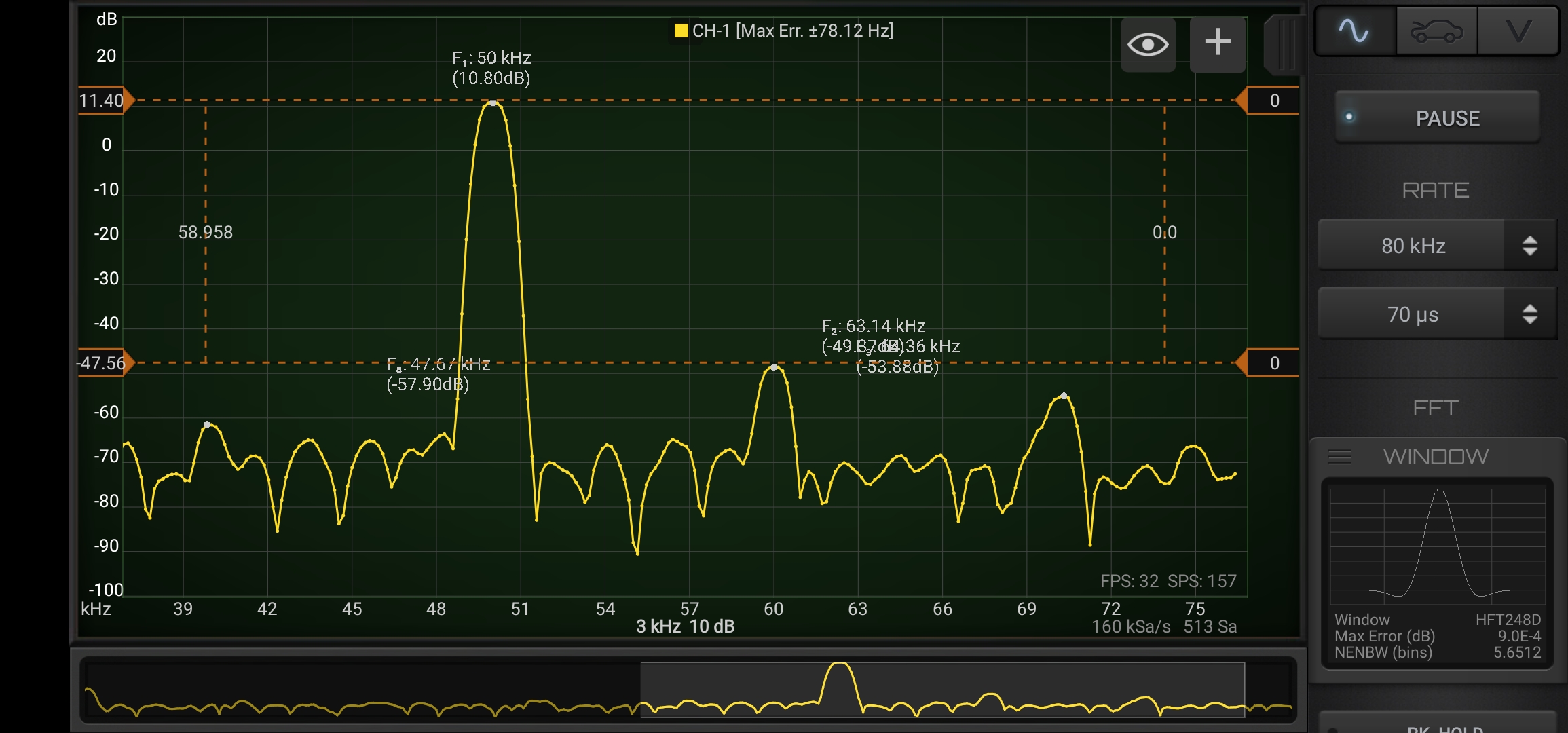
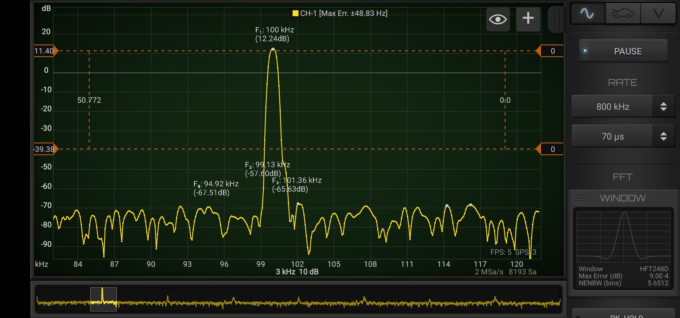
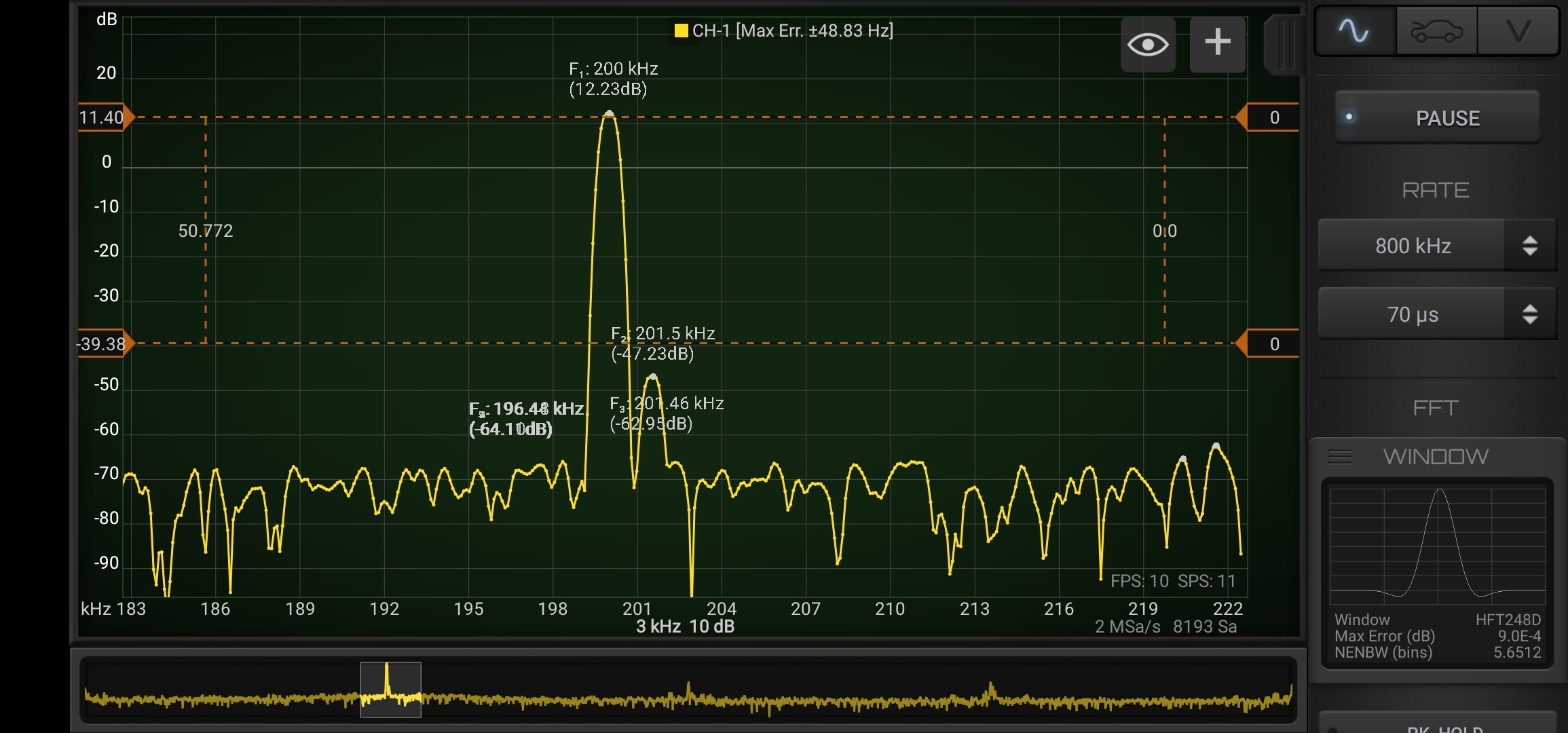
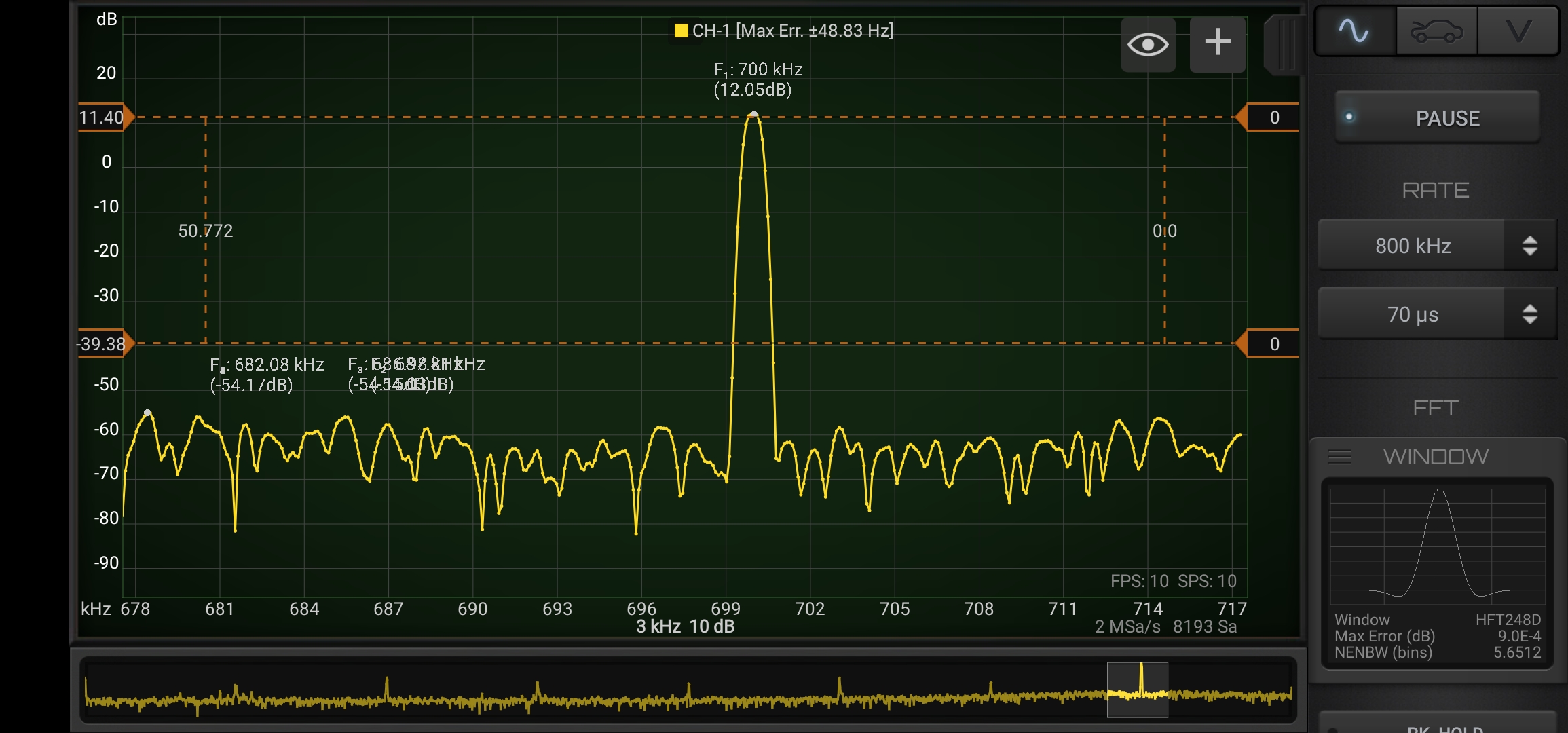
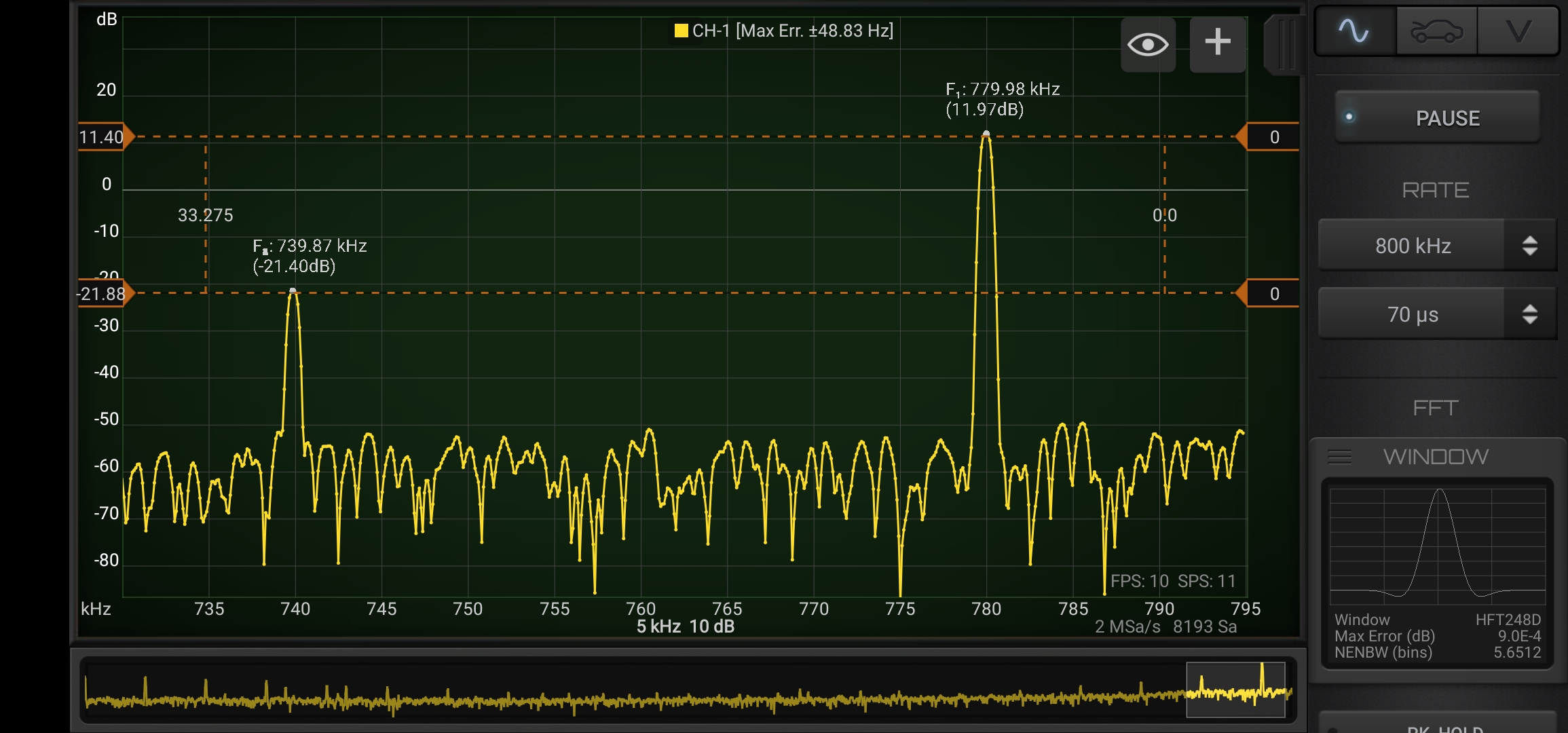
Tests with FFT
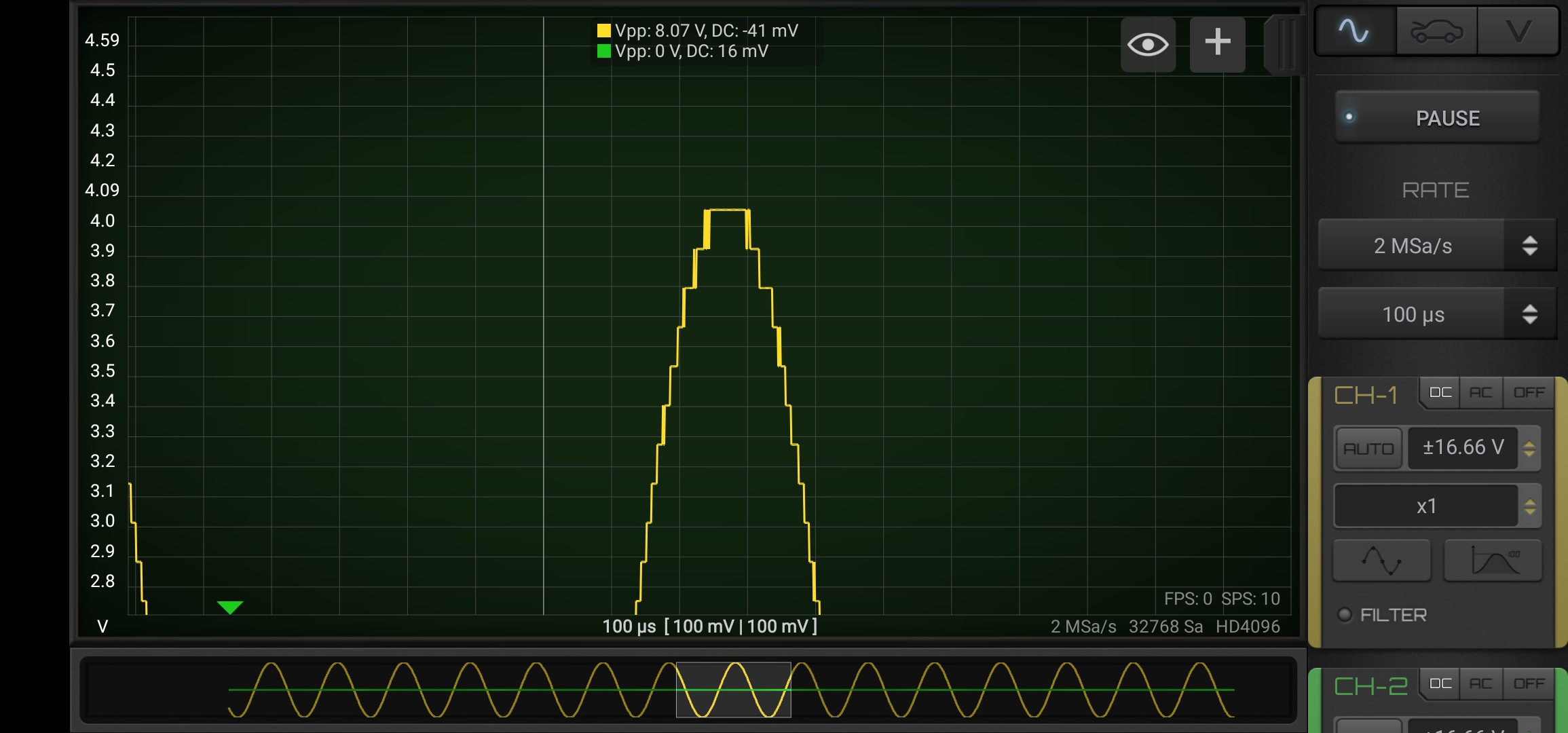
ADC 8-bit vs 9-up bits
Comparison between 8-bit ADC (provided by selecting the highest rate) and the next rate.
We use technologies like cookies to store and/or access device information. We do this to improve browsing experience and to show personalized ads. Consenting to these technologies will allow us to process data such as browsing behavior or unique IDs on this site. Not consenting or withdrawing consent, may adversely affect certain features and functions.
Functional
Always active
The technical storage or access is strictly necessary for the legitimate purpose of enabling the use of a specific service explicitly requested by the subscriber or user, or for the sole purpose of carrying out the transmission of a communication over an electronic communications network.
Preferences
The technical storage or access is necessary for the legitimate purpose of storing preferences that are not requested by the subscriber or user.
Statistics
The technical storage or access that is used exclusively for statistical purposes.The technical storage or access that is used exclusively for anonymous statistical purposes. Without a subpoena, voluntary compliance on the part of your Internet Service Provider, or additional records from a third party, information stored or retrieved for this purpose alone cannot usually be used to identify you.
Marketing
The technical storage or access is required to create user profiles to send advertising, or to track the user on a website or across several websites for similar marketing purposes.